 ALLPCB


Advanced Driver Assistance Systems (ADAS) are transforming the automotive industry, making vehicles safer and smarter. At the heart of these systems are high-density printed circuit boards (PCBs) that power complex functionalities like lane departure warnings, adaptive cruise control, and automated parking. However, manufacturing these high-density PCBs for ADAS comes with significant challenges, from intricate designs to strict reliability standards. In this blog, we’ll explore how to overcome these hurdles in PCB manufacturing, focusing on high-density PCBs, ADAS, automotive applications, microvias, SMT assembly, and DFM (Design for Manufacturability). Let’s dive into the solutions that ensure quality and performance in this demanding field.
What Are High-Density PCBs and Why Are They Critical for ADAS?
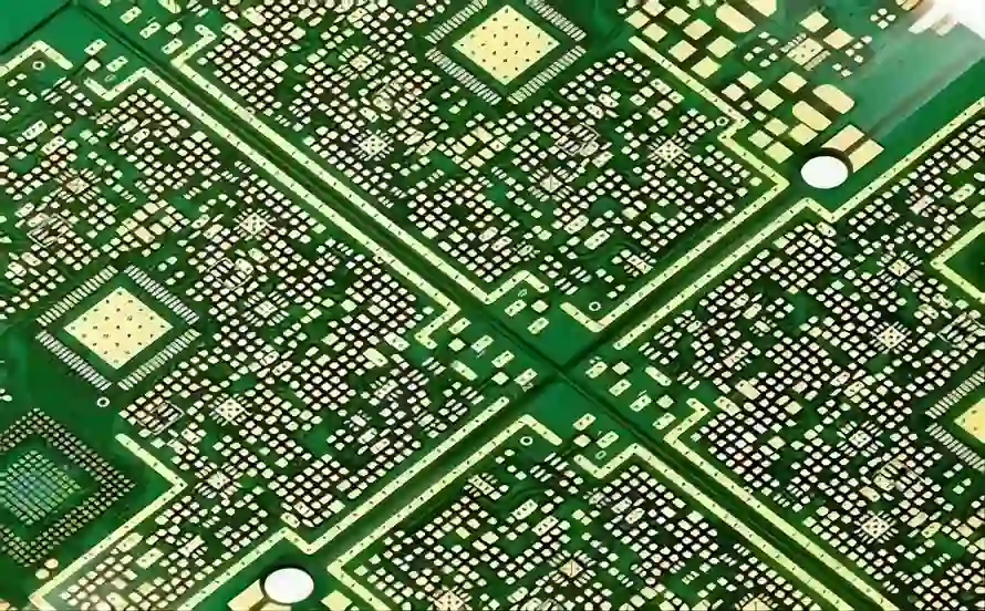
High-density PCBs are circuit boards designed with a high number of components and connections packed into a small area. They often feature fine lines (as narrow as 3 mils or 0.075 mm), tight spacing, and multiple layers—sometimes exceeding 20 layers in automotive applications. For ADAS, these boards are essential because they support the integration of sensors, cameras, radar systems, and processing units that require fast signal transmission and minimal noise interference.
In automotive environments, high-density PCBs must withstand harsh conditions like temperature fluctuations (from -40°C to 85°C), vibrations, and humidity while maintaining signal integrity at high frequencies (often in the GHz range for radar systems). Failing to address manufacturing challenges can lead to performance issues or safety risks, making it vital to tackle these obstacles head-on.
Key Manufacturing Challenges for High-Density ADAS PCBs
Creating PCBs for ADAS involves overcoming several technical barriers. Below, we break down the most common challenges in PCB manufacturing and how they impact production.
1. Complexity of Design and Miniaturization
ADAS systems demand compact designs to fit into tight spaces within vehicles. This requires miniaturization, achieved through high-density PCBs with fine traces and small vias. For example, trace widths below 4 mils and spacing under 3 mils are common, pushing the limits of standard fabrication processes. Misalignment or defects at this scale can cause signal crosstalk or short circuits, compromising the system’s reliability.
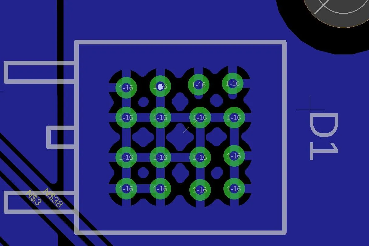
2. Reliability of Microvias in Harsh Environments
Microvias, tiny holes (often less than 6 mils or 0.15 mm in diameter) drilled by lasers, are critical for connecting layers in high-density PCBs. They allow for more connections in less space but are prone to failure under thermal stress or vibration—common in automotive settings. Cracks or voids in microvias can disrupt signal paths, leading to system failures in ADAS applications where uptime is non-negotiable.
3. Signal Integrity at High Frequencies
ADAS components like radar and LiDAR operate at high frequencies, requiring PCBs to maintain signal integrity with minimal loss. Impedance mismatches—often caused by inconsistent dielectric materials or poor trace geometry—can degrade performance. For instance, a typical radar system operating at 77 GHz demands impedance control within ±5% to avoid signal distortion.
4. Thermal Management Issues
High-density PCBs in ADAS generate significant heat due to closely packed components and high processing power. Without proper thermal management, temperatures can exceed safe limits, affecting component lifespan. Automotive standards often require PCBs to handle continuous operation at 85°C, making heat dissipation a critical design and manufacturing concern.
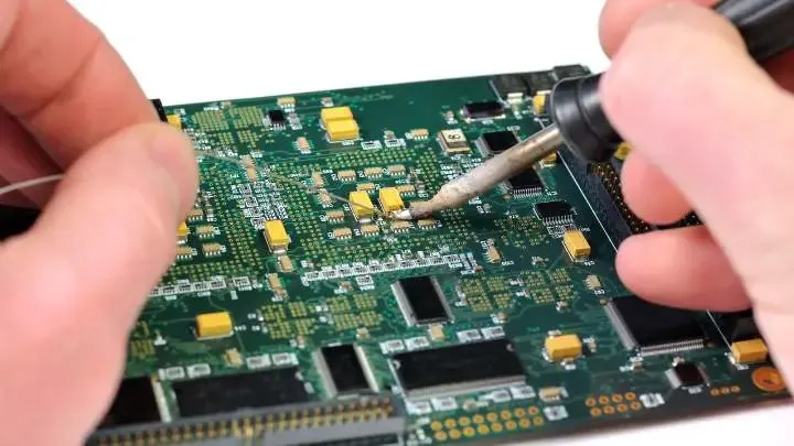
5. SMT Assembly Precision
SMT assembly (Surface Mount Technology) is the go-to method for placing components on high-density PCBs. However, the small size of components (like 0201 or 01005 packages, measuring just 0.6 mm x 0.3 mm or smaller) demands extreme precision. Misplacement by even 0.1 mm can lead to soldering defects or connection failures, especially under the vibrations of a moving vehicle.
Strategies to Overcome Manufacturing Challenges
Addressing these challenges requires a combination of advanced techniques, careful planning, and adherence to best practices in PCB manufacturing. Here’s how to ensure success when producing high-density PCBs for ADAS.
1. Leverage Design for Manufacturability (DFM) Principles
DFM (Design for Manufacturability) is a proactive approach to designing PCBs that are easier and more cost-effective to produce without sacrificing quality. For ADAS PCBs, DFM includes:
- Ensuring trace widths and spacing align with fabrication capabilities (e.g., maintaining at least 3.5 mils for standard processes).
- Optimizing via placement to avoid stress points, reducing the risk of microvia failure.
- Selecting materials with consistent dielectric properties to maintain impedance control, such as high-frequency laminates with a dielectric constant (Dk) of around 3.0 to 3.5 for radar applications.
By incorporating DFM early in the design phase, manufacturers can minimize costly revisions and improve yield rates.
2. Enhance Microvia Reliability with Advanced Processes
To prevent microvia failures, manufacturers can adopt advanced techniques like:
- Using laser drilling for precise microvia formation, ensuring diameters as small as 4 mils with aspect ratios below 0.75:1 to avoid plating issues.
- Implementing stacked or staggered microvia structures instead of through-hole vias to reduce thermal stress.
- Applying rigorous testing, such as thermal cycling between -40°C and 125°C, to simulate automotive conditions and identify weak points.
These methods improve the durability of microvias, ensuring they withstand the harsh automotive environment.
3. Optimize Signal Integrity with Material and Design Choices
Maintaining signal integrity in high-density PCBs for ADAS involves careful selection of materials and design adjustments:
- Choose low-loss materials with a dissipation factor (Df) below 0.005 to minimize signal attenuation at high frequencies like 77 GHz.
- Design controlled impedance traces with tools to simulate signal behavior, targeting a tolerance of ±5% for critical paths.
- Use ground planes and shielding to reduce electromagnetic interference (EMI), which is crucial for noise-sensitive ADAS systems.
These steps ensure reliable data transmission, even in compact, high-speed designs.
4. Improve Thermal Management in Design and Fabrication
Effective thermal management is vital for high-density PCBs in ADAS. Consider these strategies:
- Incorporate thermal vias (small holes filled with conductive material) near heat-generating components to transfer heat to outer layers or heat sinks.
- Use high-thermal-conductivity materials, such as metal-core PCBs, for better heat dissipation.
- Design layouts to space out high-power components, preventing localized hotspots that could exceed 100°C.
By addressing heat early in the design phase, manufacturers can extend the lifespan of ADAS systems.
5. Ensure Precision in SMT Assembly
For flawless SMT assembly, precision and quality control are non-negotiable:
- Utilize automated pick-and-place machines with vision systems to achieve placement accuracy within 0.05 mm for tiny components like 01005 packages.
- Apply solder paste inspection (SPI) to verify paste volume and alignment before reflow soldering, reducing defects like tombstoning or bridging.
- Conduct X-ray inspection post-assembly to detect hidden solder joint issues, especially under dense component areas.
These measures ensure robust connections, critical for the reliability of ADAS systems under constant vibration.
Meeting Automotive Standards for ADAS PCBs
Beyond technical challenges, high-density PCBs for automotive ADAS must comply with strict industry standards like ISO 26262 for functional safety and AEC-Q100 for component reliability. These standards mandate rigorous testing, including:
- Thermal shock tests to ensure performance across temperature extremes (-40°C to 85°C).
- Vibration tests simulating road conditions, often at frequencies up to 200 Hz with accelerations of 5g or more.
- Humidity resistance tests to prevent corrosion or delamination in high-moisture environments.
Manufacturers must integrate these requirements into their processes, from material selection to final inspection, to deliver PCBs that meet automotive-grade expectations.
Future Trends in High-Density ADAS PCB Manufacturing
As ADAS technology evolves, so do the demands on PCB manufacturing. Emerging trends include:
- Advanced Materials: Adoption of glass core substrates for better thermal and mechanical stability, with market growth projected to reach significant value by 2030, according to industry reports.
- Higher Integration: Increased use of System-in-Package (SiP) solutions to combine multiple functions into a single, compact module.
- Automation: Greater reliance on AI-driven design tools and robotic assembly to enhance precision and reduce human error in SMT assembly.
Staying ahead of these trends ensures manufacturers are prepared for the next generation of ADAS innovations.
Conclusion: Building Reliable High-Density PCBs for ADAS
Manufacturing high-density PCBs for ADAS in the automotive industry is no small feat. Challenges like design complexity, microvia reliability, signal integrity, thermal management, and SMT assembly precision require innovative solutions and strict adherence to standards. By embracing DFM principles, leveraging advanced processes, and focusing on quality at every step, manufacturers can overcome these obstacles and deliver PCBs that power safer, smarter vehicles.
At ALLPCB, we’re committed to supporting engineers and designers in navigating the complexities of PCB manufacturing for high-density PCBs. With expertise in cutting-edge techniques and a focus on reliability, we help bring ADAS innovations to life. Whether you’re tackling microvia challenges or optimizing for high-frequency signals, the right strategies and partnerships can make all the difference in achieving success.


