 ALLPCB


In the world of PCB manufacturing, precision is everything. One key element that ensures accuracy during automated assembly is the strategic placement of fiducial marks on panels. But what exactly is fiducial mark placement, and how can optimizing it enhance PCB manufacturing? In this detailed guide, we’ll dive into the importance of panel fiducial best practices, explore SMT placement techniques, and provide actionable tips for PCB manufacturing optimization, especially in high component density designs.
Whether you’re a design engineer or a manufacturing professional, understanding how to place fiducial marks effectively can significantly improve assembly accuracy and reduce errors. Let’s explore how to master fiducial mark placement for better results in surface mount technology (SMT) processes.
What Are Fiducial Marks and Why Do They Matter in PCB Manufacturing?
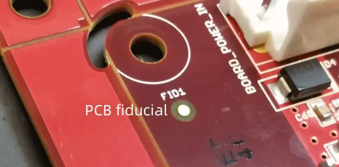
Fiducial marks are small, typically circular copper pads on a PCB or panel that serve as reference points for automated assembly machines. These marks help pick-and-place machines identify the exact orientation and position of the board during SMT assembly. Without accurate fiducial placement, machines may misalign components, leading to costly errors and rework.
In PCB manufacturing optimization, fiducial marks are critical because they ensure that every component, no matter how small or densely packed, is placed with precision. For instance, in high component density designs, even a slight misalignment of 0.1 mm can cause a component to fail or short-circuit. Fiducial marks act as a guide, allowing machines to adjust for any slight variations in board positioning on the assembly line.
The Role of Panel Fiducial Placement in SMT Assembly
Panel fiducial placement refers to the positioning of fiducial marks on a panelized PCB layout, where multiple boards are arranged together for efficient manufacturing. Proper placement of these marks ensures that the assembly machine can recognize the panel’s orientation and align components accurately across all boards in the panel.
In SMT placement techniques, fiducial marks are typically categorized into two types:
- Global Fiducials: These are placed on the panel to provide a reference for the entire set of boards. They help the machine understand the panel’s overall orientation.
- Local Fiducials: These are placed near specific components or high-density areas on individual boards within the panel. They ensure precision for intricate or critical placements.
By using both global and local fiducials, manufacturers can achieve a higher degree of accuracy. For example, in a panel with 10 individual PCBs, having at least three global fiducials (one near each corner of the panel) can reduce rotational errors to less than 0.01 degrees during assembly.
Best Practices for Panel Fiducial Placement
Implementing panel fiducial best practices can make a significant difference in the efficiency and accuracy of your PCB manufacturing process. Below are some key guidelines to follow for optimal fiducial mark placement:
1. Place Fiducials Asymmetrically for Orientation Clarity
To avoid confusion in board orientation, place fiducial marks in an asymmetrical pattern. For instance, position three global fiducials on a panel in a triangular layout rather than a symmetrical square. This helps the machine instantly recognize the correct orientation, reducing the risk of a 180-degree misalignment.
2. Maintain Adequate Spacing from Board Edges
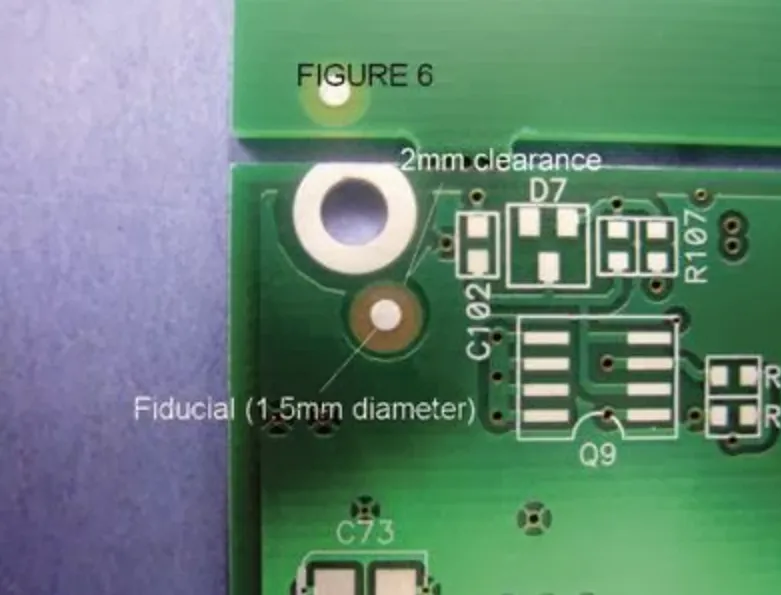
Fiducial marks should be placed at least 5 mm away from the panel edges to avoid interference with tooling holes or rails used during manufacturing. If placed too close, the marks may be obscured or damaged, leading to machine errors.
3. Use Proper Size and Shape for Fiducial Marks
The size of fiducial marks typically ranges from 1 mm to 3 mm in diameter, with a surrounding clearance area (free of solder mask) at least twice the diameter of the mark. A round shape is preferred as it provides a clear center point for machine vision systems to lock onto.
4. Incorporate Local Fiducials for High Component Density Areas
In designs with high component density, such as those with BGA (Ball Grid Array) components, local fiducials are essential. Place these marks near the component (within 10 mm) to ensure the machine can fine-tune its alignment for that specific area. For example, a BGA with a pitch of 0.5 mm requires placement accuracy within 0.05 mm, which local fiducials help achieve.
5. Avoid Placing Fiducials Near High-Noise Areas
Keep fiducial marks away from areas with heavy copper traces or components that may interfere with the machine’s vision system. Reflections or shadows from nearby elements can confuse the system, so ensure a clear, unobstructed view of each mark.
How Fiducial Mark Placement Impacts PCB Manufacturing Optimization
Optimizing fiducial mark placement directly contributes to PCB manufacturing optimization by minimizing errors and speeding up the assembly process. Here’s how:
Reducing Assembly Errors
Accurate fiducial placement reduces the likelihood of component misalignment, which is a common issue in SMT assembly. Misalignment errors can cost manufacturers thousands of dollars in rework and scrap. For instance, a 1% error rate in component placement on a batch of 10,000 boards can result in 100 defective units, each potentially costing $50 or more to repair.
Improving Throughput
Well-placed fiducials allow machines to quickly recognize board orientation and proceed with component placement without delays. This can increase throughput by up to 20%, especially in high-volume production runs where every second counts.
Enhancing Compatibility with Advanced SMT Placement Techniques
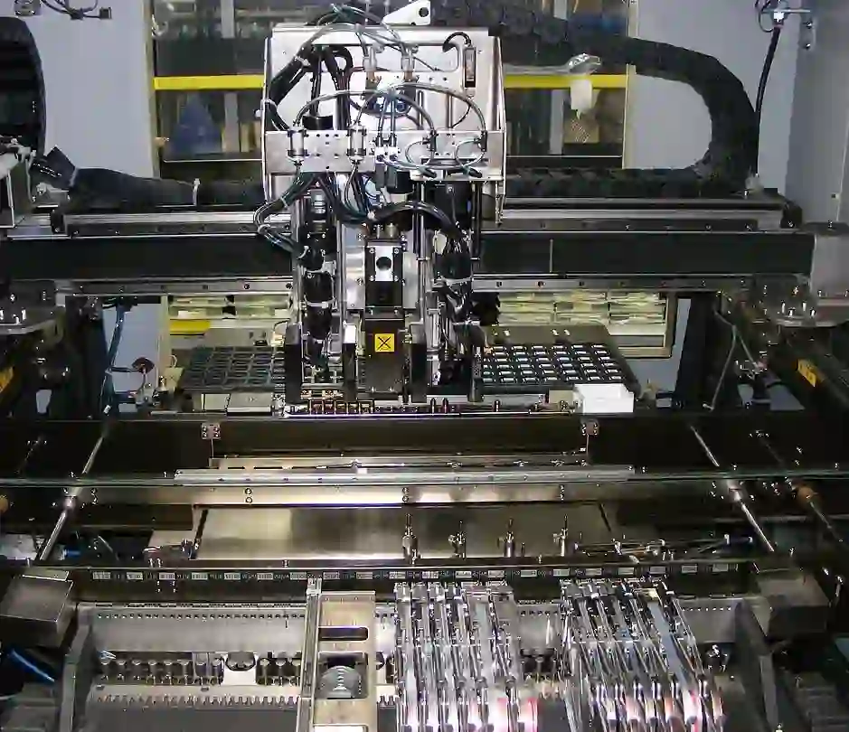
Modern SMT placement techniques, such as high-speed pick-and-place systems, rely heavily on fiducial marks for calibration. Optimized placement ensures compatibility with these advanced systems, enabling manufacturers to handle complex designs with tighter tolerances.
Challenges in Fiducial Placement for High Component Density Designs
High component density designs pose unique challenges for fiducial mark placement. With components packed closely together, there’s often limited space for fiducials, and the risk of misalignment increases. Here are some common challenges and solutions:
Limited Space on the Board
In densely populated designs, finding room for fiducial marks can be tough. To address this, prioritize local fiducials near critical components like fine-pitch ICs, even if it means reducing the number of marks elsewhere. A single well-placed local fiducial near a critical area can be more effective than multiple poorly positioned ones.
Increased Risk of Vision System Errors
With components and traces crowded together, machine vision systems may struggle to detect fiducial marks due to reflections or obstructions. To mitigate this, ensure a clear contrast between the fiducial mark (bare copper) and the surrounding area (solder mask). A clearance area of at least 3 mm around the mark can help.
Balancing Fiducial Placement with Design Constraints
Designers must balance the need for fiducials with other layout requirements, such as signal integrity and thermal management. For example, placing a fiducial mark too close to a high-frequency trace (operating at 5 GHz) may introduce noise or interference. Careful planning during the design phase can help avoid such conflicts.
Advanced Tips for Panel Fiducial Best Practices
For those looking to take their fiducial placement strategy to the next level, consider these advanced tips:
Simulate Machine Vision During Design
Use design software to simulate how a machine vision system will detect fiducial marks on your panel. This can help identify potential issues, such as marks that are too close to reflective components or areas with poor contrast, before the board goes into production.
Collaborate with Your Manufacturing Partner
Work closely with your manufacturing team to understand their specific requirements for fiducial placement. Different assembly lines may have unique machine vision systems or calibration needs, so aligning your design with their capabilities can prevent delays and errors.
Test and Iterate Fiducial Placement
During prototype runs, test different fiducial placements to determine which configuration yields the best assembly accuracy. For instance, if local fiducials near a BGA component result in a placement accuracy of 99.9%, but moving them 5 mm closer increases it to 99.95%, that small adjustment could save significant costs in high-volume production.
The Future of Fiducial Marks in PCB Manufacturing
As PCB manufacturing technology evolves, the role of fiducial marks remains crucial, even with advancements in machine vision and automation. While some modern systems can use component outlines or other features for alignment, fiducial marks provide a reliable, standardized reference point that ensures consistency across different machines and manufacturers.
In the future, we may see innovations like embedded fiducial marks or digital calibration systems that reduce the need for physical copper pads. However, for now, optimizing panel fiducial placement remains a cornerstone of efficient and accurate PCB assembly, especially for complex, high-density designs.
Conclusion: Mastering Fiducial Mark Placement for Better PCB Outcomes
Optimizing panel fiducial placement is a powerful way to enhance PCB manufacturing efficiency and accuracy. By following panel fiducial best practices, leveraging SMT placement techniques, and addressing the challenges of high component density, designers and manufacturers can achieve better results with fewer errors.
From placing fiducials asymmetrically to using local marks for critical areas, every decision in fiducial mark placement plays a role in PCB manufacturing optimization. As you design your next panel, keep these strategies in mind to ensure a smoother assembly process and higher-quality boards.
With the right approach to fiducial placement, you can reduce costs, improve throughput, and deliver reliable, high-performance PCBs that meet the demands of today’s advanced electronics. Let’s build with precision and efficiency, one fiducial mark at a time.


