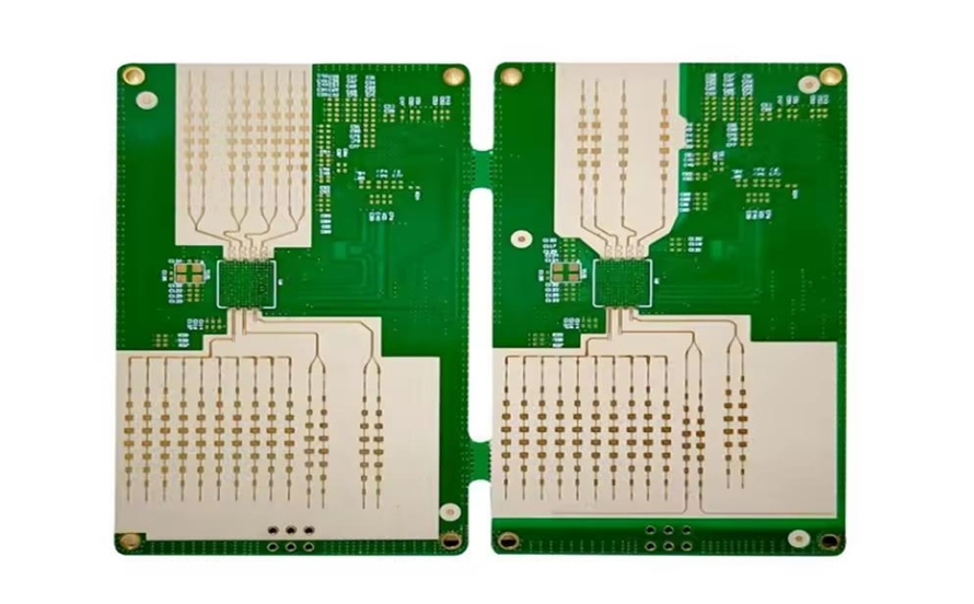
If you're designing a high-current printed circuit board (PCB), one of the most critical factors to consider is the outer layer copper weight. But what is the ideal copper weight for your design, and how do you optimize it for performance and reliability? In short, optimizing outer layer copper weight involves selecting a thickness (often measured in ounces per square foot, or oz/ft2) that balances current carrying capacity, heat dissipation, and manufacturing constraints. For high-current applications, 2 oz/ft2 or higher is often recommended, depending on the current load and trace width.
In this comprehensive guide, we'll dive deep into the nuances of PCB outer layer copper thickness, high-current PCB design, and PCB power layer design. We'll also walk you through outer layer copper weight calculation and explain how to determine the PCB current carrying capacity for your specific needs. Whether you're an engineer or a designer, this post will equip you with actionable insights to enhance your PCB projects.
Why Outer Layer Copper Weight Matters in High-Current PCB Design
When designing PCBs for high-current applications, such as power supplies, motor controllers, or automotive electronics, the copper weight on the outer layers plays a pivotal role. Copper weight refers to the thickness of the copper foil on the PCB, typically measured in ounces per square foot (oz/ft2). A 1 oz/ft2 copper layer is approximately 35 micrometers (μm) thick, while 2 oz/ft2 is around 70 μm.
The primary reason copper weight matters is its direct impact on the board's ability to handle high currents without overheating. Thicker copper can carry more current and dissipate heat more effectively, reducing the risk of trace burnout or delamination. However, thicker copper also increases manufacturing costs and can pose challenges in fine-pitch designs. Striking the right balance is key to a successful high-current PCB design.

Understanding PCB Current Carrying Capacity
Before diving into copper weight optimization, it's essential to grasp the concept of PCB current carrying capacity. This refers to the maximum amount of current a trace can handle without exceeding a safe temperature rise. The current carrying capacity depends on several factors, including trace width, copper thickness, ambient temperature, and the allowable temperature rise (often set at 10°C or 20°C for safety).
For instance, a 10-mil-wide trace with 1 oz/ft2 copper can typically handle about 1 ampere (A) of current with a 10°C temperature rise. However, if you increase the copper weight to 2 oz/ft2, the same trace can handle roughly double the current, around 2 A, under similar conditions. Wider traces also improve current capacity—a 50-mil trace with 1 oz/ft2 copper can handle closer to 3-4 A.
These values are based on industry standards like IPC-2221, which provides guidelines for trace sizing. However, real-world applications may vary due to factors like heat dissipation through nearby components or airflow. Using simulation tools or referencing detailed charts can help ensure accuracy in your design.
How to Calculate Outer Layer Copper Weight for Your PCB
Performing an outer layer copper weight calculation is a critical step in designing a PCB for high-current applications. Here's a simplified process to determine the right copper weight:
- Determine the Required Current: Identify the maximum current your traces will carry. For example, if you're designing a power supply circuit that needs to handle 5 A, this is your starting point.
- Estimate Temperature Rise: Decide on an acceptable temperature rise for your application. A 10°C rise is common for most designs to ensure reliability.
- Select Trace Width: Using a current carrying capacity chart or calculator (based on IPC standards), find the trace width needed for your current and temperature rise at a standard copper weight (e.g., 1 oz/ft2). For 5 A, you might need a 100-mil-wide trace at 1 oz/ft2.
- Adjust Copper Weight: If the required trace width is impractical due to space constraints, consider increasing the copper weight to 2 oz/ft2 or higher. Doubling the copper thickness roughly doubles the current capacity, so a 50-mil trace at 2 oz/ft2 could handle the same 5 A.
- Verify Heat Dissipation: Ensure that the thicker copper won't cause excessive heat buildup in other areas of the board. Thermal vias or heat sinks may be necessary.
This method provides a starting point, but always validate your calculations with PCB design software or consult with your manufacturing partner to account for specific constraints.
Best Practices for PCB Power Layer Design in High-Current Applications
In addition to optimizing outer layer copper weight, effective PCB power layer design is crucial for high-current PCBs. Power layers are typically internal layers dedicated to distributing power and ground signals, but the principles can also apply to outer layers in simpler designs. Here are some best practices to follow:
- Use Thicker Copper for Power Planes: Similar to outer layers, power planes benefit from thicker copper (e.g., 2 oz/ft2 or more) to minimize voltage drops and improve current distribution. For a design handling 10 A, a 2 oz/ft2 power plane can reduce resistance significantly compared to 1 oz/ft2.
- Minimize Trace Lengths: Shorter traces reduce resistance and heat generation. Position high-current components closer to power sources to keep paths short.
- Incorporate Thermal Vias: Use thermal vias to transfer heat from high-current areas to other layers or heat sinks. For example, placing vias under a high-power component can lower the temperature by 5-10°C.
- Balance Copper Distribution: Uneven copper distribution can cause warping during manufacturing. If one layer has heavy copper, balance it with similar weights on other layers or use copper thieving (unused copper areas) to maintain symmetry.
By integrating these strategies, you can ensure that your power layer design supports the demands of high-current applications while maintaining board integrity.
Choosing the Right PCB Outer Layer Copper Thickness
Selecting the appropriate PCB outer layer copper thickness involves weighing several factors beyond just current capacity. Here's what to consider:
- Current Requirements: As discussed, higher currents demand thicker copper. For applications exceeding 3-5 A per trace, start with at least 2 oz/ft2 and scale up as needed.
- Board Size and Space: Thicker copper allows narrower traces for the same current, which is helpful in compact designs. However, manufacturing limitations may restrict trace widths with very thick copper (e.g., 3 oz/ft2 or 4 oz/ft2).
- Cost: Thicker copper increases material and processing costs. For example, moving from 1 oz/ft2 to 2 oz/ft2 can raise costs by 20-30%, with even higher jumps for 3 oz/ft2 or more.
- Manufacturing Capabilities: Not all manufacturers can handle very thick copper (above 3 oz/ft2) without special processes. Confirm with your fabrication partner before finalizing your design.
- Thermal Management: While thicker copper dissipates heat better, it can also retain heat in confined areas. Pair it with proper ventilation or heat sinks for optimal performance.
For most high-current designs, starting with 2 oz/ft2 is a safe choice, providing a good balance of performance and cost. However, for extreme applications like electric vehicle battery management systems, copper weights of 3-4 oz/ft2 or even custom solutions may be necessary.

Common Challenges and Solutions in High-Current PCB Design
Designing PCBs for high-current applications often comes with unique challenges. Here are some common issues related to copper weight and how to address them:
- Overheating: If traces overheat despite using thicker copper, consider adding heat sinks or increasing airflow around the board. For a design with a hotspot reaching 50°C above ambient, a small heat sink can drop this by 15-20°C.
- Space Constraints: When board space limits trace width, opt for thicker copper or use multiple layers to split the current load. For instance, a 5 A load can be distributed across two 2.5 A traces on different layers.
- Manufacturing Defects: Heavy copper can lead to uneven etching or plating issues. Work closely with your manufacturer to ensure they can handle the specified copper weight without compromising quality.
- Cost Overruns: If thicker copper pushes your budget too high, explore hybrid designs where only high-current areas use heavy copper, while other sections use standard 1 oz/ft2.
Proactive planning and collaboration with your manufacturing partner can help mitigate these challenges, ensuring a reliable and cost-effective design.
Tools and Resources for Optimizing Copper Weight
To streamline the process of optimizing copper weight and trace design, several tools and resources are available:
- Current Capacity Calculators: Online tools based on IPC standards can quickly estimate the required trace width and copper thickness for a given current. These are invaluable for initial design phases.
- PCB Design Software: Advanced software often includes thermal and electrical simulation features to model current flow and heat dissipation. Use these to validate your copper weight choices.
- IPC Standards: Refer to documents like IPC-2221 for detailed guidelines on trace sizing and current carrying capacity. These standards are widely accepted in the industry.
- Manufacturer Guidelines: Your fabrication partner can provide specific recommendations based on their capabilities, especially for heavy copper designs.
Using these resources ensures that your design aligns with both theoretical best practices and practical manufacturing constraints.
Conclusion: Achieving Balance in High-Current PCB Design
Optimizing the outer layer copper weight for high-current PCBs is a critical aspect of ensuring performance, reliability, and cost-effectiveness. By understanding PCB current carrying capacity, performing accurate outer layer copper weight calculations, and following best practices for PCB power layer design, you can create boards that handle high currents without compromising on quality.
Start with a baseline of 2 oz/ft2 for most high-current applications, and adjust based on your specific current needs, thermal requirements, and budget. Always validate your design with simulations or calculators, and collaborate with your manufacturing partner to address any limitations. With the right approach to high-current PCB design and PCB outer layer copper thickness, you can achieve a robust and efficient solution for even the most demanding projects.
At ALLPCB, we're committed to supporting your PCB design journey with resources, expertise, and high-quality manufacturing services. Whether you're tackling a small prototype or a large-scale production run, we're here to help you succeed.

 ALLPCB


