 ALLPCB


When designing a printed circuit board (PCB), achieving optimal performance often hinges on understanding the relationship between copper thickness (measured in mils) and trace impedance. For engineers working on high-speed or high-frequency designs, this connection is critical to ensuring signal integrity and minimizing issues like reflections or crosstalk. In short, copper thickness directly impacts trace impedance, which in turn affects how signals travel through a PCB. Thicker copper can lower impedance, while thinner copper increases it, requiring careful calculation and design to match the desired impedance for your circuit.
In this comprehensive guide, we’ll dive deep into the nuances of PCB trace impedance, the impact of copper thickness, and how to balance these factors for superior transmission line design. Whether you’re a seasoned engineer or just starting, this post will provide actionable insights into impedance calculation and signal integrity simulation to help you maximize your PCB performance.
What Is PCB Trace Impedance and Why Does It Matter?
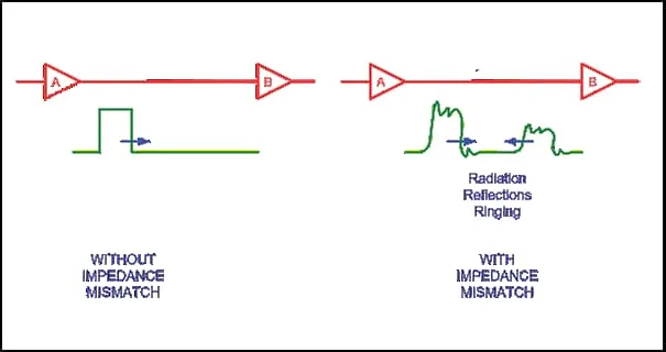
PCB trace impedance is the measure of opposition a trace offers to the flow of an alternating current (AC) signal. It combines resistance (from the copper trace) and reactance (from capacitance and inductance) and is typically expressed in ohms (Ω). In high-speed circuits, maintaining a consistent impedance—often 50Ω or 75Ω depending on the application—is crucial for preventing signal reflections, which can degrade performance or cause data errors.
Impedance matters because mismatched traces can lead to signal loss, noise, or interference. For instance, in a high-frequency design operating at 1 GHz, even a small mismatch can cause significant signal distortion. This is why understanding and controlling impedance is a cornerstone of modern PCB design, especially for applications like USB, HDMI, or RF circuits.
How Copper Thickness Impacts PCB Trace Impedance
Copper thickness, often measured in mils (1 mil = 0.001 inches) or ounces per square foot (oz/ft2), plays a significant role in determining trace impedance. Common copper thicknesses in PCB manufacturing range from 0.5 oz (0.7 mils) to 2 oz (2.8 mils), with 1 oz (1.4 mils) being the standard for many designs.
The relationship between copper thickness and impedance is inverse but nuanced. A thicker copper layer reduces the resistance of the trace, which can lower the overall impedance slightly. However, the effect is often less pronounced than other factors like trace width or dielectric material thickness. For example, increasing copper thickness from 1 oz to 2 oz might reduce impedance by only a few ohms, depending on the trace geometry and substrate properties.
Why does this matter? In high-current applications, thicker copper is often preferred to handle higher power without overheating. However, for high-frequency designs, the slight change in impedance due to copper thickness must be accounted for to avoid mismatches. If not managed properly, this can lead to signal integrity issues, especially in transmission line designs where precision is key.
Key Takeaway
While copper thickness does impact trace impedance, its effect is often secondary to trace width and dielectric properties. Still, it must be considered in impedance calculations, especially for designs pushing performance boundaries.
Impedance Calculation: Breaking Down the Factors
Calculating trace impedance involves several variables beyond just copper thickness. The most common formula used for microstrip traces (traces on the outer layer of a PCB) is derived from transmission line theory. Here’s a simplified version of the characteristic impedance (Z?) formula for a microstrip:
Z? = (87 / √(εr + 1.41)) * ln(5.98 * h / (0.8 * w + t))
Where:
- Z? = Characteristic impedance (ohms)
- εr = Dielectric constant of the substrate material (e.g., 4.5 for FR-4)
- h = Height of the dielectric between the trace and ground plane (mils)
- w = Width of the trace (mils)
- t = Thickness of the copper trace (mils)
From this formula, you can see that copper thickness (t) has a direct but relatively small influence on impedance compared to trace width (w) and dielectric height (h). For instance, in a typical design with a 1 oz copper trace (1.4 mils thick), a trace width of 10 mils, and a dielectric height of 8 mils on FR-4 material, the impedance might be around 50Ω. Doubling the copper thickness to 2 oz (2.8 mils) might decrease the impedance by only 1-2Ω, assuming other factors remain constant.
This calculation shows that while copper thickness matters, it’s often a fine-tuning parameter rather than a primary driver of impedance. Engineers typically adjust trace width or choose specific dielectric materials to hit the target impedance more effectively.
Practical Example
Consider a high-speed USB 3.0 design requiring a differential impedance of 90Ω. Using a standard 1 oz copper thickness, you might set the trace width to 6 mils and spacing to 8 mils on a 4-layer board with a dielectric height of 10 mils. If you switch to a 2 oz copper thickness for better current handling, the impedance might drop to 88Ω. While this is within tolerance for many designs, precision applications may require recalculating trace width or dielectric properties to compensate.
Transmission Line Design: Balancing Copper Thickness and Impedance
In transmission line design, the goal is to create a uniform path for signals to travel with minimal loss or reflection. Copper thickness impacts this by influencing both impedance and current-carrying capacity. Thicker copper can reduce resistive losses, which is beneficial for long traces or high-current paths, but it also slightly alters impedance, as discussed earlier.
For high-speed designs, such as those operating above 100 MHz, maintaining consistent impedance along the entire trace is critical. This means considering not just copper thickness but also trace width, dielectric material, and the proximity to ground planes. A common approach is to use a stack-up configuration with controlled dielectric heights and copper weights to achieve the desired impedance.
For example, in a 4-layer PCB, you might use 1 oz copper on all layers for cost-effectiveness. However, if the inner layers carry high-current signals, opting for 2 oz copper on those layers could reduce heat buildup, even if it requires slight adjustments to trace geometry to maintain impedance.
Best Practice
Always simulate your transmission line design using specialized software to predict impedance and signal behavior. Tools for signal integrity simulation can model how changes in copper thickness affect performance, allowing you to make informed decisions before fabrication.
Signal Integrity Simulation: Predicting Performance with Copper Thickness
Signal integrity simulation is a powerful way to test how copper thickness and trace impedance interact in real-world scenarios. These simulations analyze factors like signal reflections, crosstalk, and timing issues, providing a virtual testbed for your PCB design.
During simulation, you can input different copper thicknesses to see their impact on impedance and signal quality. For instance, a simulation might reveal that a 1 oz copper trace at 50Ω impedance experiences acceptable signal loss at 500 MHz, but switching to 0.5 oz copper increases loss due to higher resistance, even if impedance remains similar. This insight helps you choose the right copper weight for your specific application.
Modern simulation tools also allow you to model skin effect—a phenomenon where high-frequency signals travel primarily on the surface of a conductor. Thicker copper provides more surface area, potentially reducing skin effect losses, but the benefit diminishes beyond a certain point (typically around 2 oz for most frequencies below 1 GHz).
Practical Tip
Start with standard copper thickness (1 oz) for most designs and use simulation to determine if a thicker layer is necessary. This approach balances cost and performance, as thicker copper increases manufacturing expenses without always delivering proportional benefits to signal integrity.
Practical Guidelines for Optimizing Copper Thickness in PCB Design
Balancing copper thickness with trace impedance requires a strategic approach. Here are some actionable guidelines to help you optimize your PCB design:
- Start with Standard Thickness: Use 1 oz copper as a baseline for most designs. It’s cost-effective and suitable for a wide range of applications, from low-frequency to moderate high-speed circuits.
- Prioritize Impedance Control: Focus on trace width and dielectric properties to hit your target impedance. Adjust copper thickness only if necessary for current handling or specific performance needs.
- Simulate Before Fabrication: Use signal integrity simulation tools to model the impact of copper thickness on impedance and signal behavior. This can save time and cost by identifying issues before production.
- Consider Application Needs: For high-current designs, thicker copper (e.g., 2 oz) may be essential to prevent overheating, even if it requires slight impedance adjustments. For high-frequency designs, prioritize uniform impedance over thickness.
- Account for Manufacturing Tolerances: Copper thickness can vary slightly during fabrication. Work with your manufacturer to ensure the final thickness matches your design specifications, especially for precision impedance control.
Common Challenges and Solutions in Managing Copper Thickness and Impedance
Designing with copper thickness and impedance in mind isn’t always straightforward. Here are some common challenges and how to address them:
Challenge 1: Impedance Mismatch Due to Thickness Variation
Small variations in copper thickness during manufacturing can shift impedance outside acceptable limits. To mitigate this, design with a small buffer (e.g., target 48-52Ω for a 50Ω requirement) and collaborate closely with your manufacturer for tight control over copper weight.
Challenge 2: Cost vs. Performance Trade-Off
Thicker copper improves current handling but increases production costs. Evaluate whether the performance gain justifies the expense. Often, optimizing trace width or layout can achieve similar results at a lower cost.
Challenge 3: High-Frequency Signal Loss
At very high frequencies (above 1 GHz), skin effect and dielectric losses overshadow the benefits of thicker copper. Focus on selecting low-loss dielectric materials and maintaining precise trace geometry rather than relying solely on copper thickness.
Conclusion: Mastering Copper Thickness for Optimal PCB Performance
The relationship between copper thickness and PCB trace impedance is a critical factor in maximizing circuit performance, especially for high-speed and high-frequency applications. While thicker copper can reduce resistance and handle higher currents, its impact on impedance is often subtle compared to trace width or dielectric properties. By understanding this balance and leveraging tools like impedance calculation and signal integrity simulation, you can design PCBs that deliver reliable, high-quality performance.
Whether you’re working on a simple prototype or a complex multilayer board, always consider copper thickness as part of your broader transmission line design strategy. With careful planning and simulation, you can fine-tune your PCB to meet the exact needs of your application, ensuring robust signal integrity and long-term reliability.


