 ALLPCB


In the world of high-current PCB design, maximizing the current carrying capacity of plated through-holes (PTH) is a critical challenge. Whether you're working on power electronics, automotive systems, or industrial applications, ensuring that PTHs can handle high currents without overheating or failing is essential. This blog post dives deep into techniques and best practices for increasing PTH current capacity, focusing on key aspects like PTH current rating, PTH copper plating thickness, and thermal management in PTH design. We'll provide actionable insights to help you optimize your PCB layouts for reliability and performance.
What Are Plated Through-Holes (PTH) and Why Do They Matter?
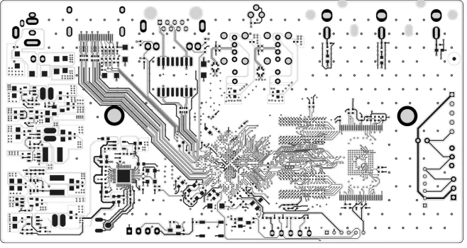
Plated through-holes (PTH) are holes drilled through a printed circuit board (PCB) and coated with a conductive layer, typically copper, to connect different layers of the board or mount through-hole components. Unlike non-plated through-holes, PTHs provide electrical connectivity and mechanical strength, making them vital for high-current applications. Their ability to carry current without degrading or causing thermal issues directly impacts the overall performance and safety of a PCB.
In high-current PCB design, PTHs often serve as the conduit for significant power delivery. If not designed properly, they can become bottlenecks, leading to excessive heat buildup, voltage drops, or even board failure. Understanding how to maximize their current carrying capacity is key to creating robust and efficient designs.

Factors Affecting PTH Current Rating
The PTH current rating, or the maximum current a plated through-hole can safely carry, depends on several interrelated factors. Let’s break them down to understand how each contributes to current capacity and how you can optimize them.
1. PTH Copper Plating Thickness
The thickness of the copper plating inside the through-hole plays a major role in determining its current carrying capacity. Thicker copper plating reduces electrical resistance, allowing more current to flow without generating excessive heat. Standard PTH copper plating thickness often ranges from 0.8 to 1.2 mils (20 to 30 micrometers) for typical boards, but for high-current applications, increasing this to 2 mils (50 micrometers) or more can significantly improve performance.
Keep in mind that thicker plating also improves durability during thermal cycling, as it can better withstand the expansion and contraction caused by temperature changes. However, increasing copper thickness may raise manufacturing costs, so balance this with your project’s budget and requirements.
2. Hole Diameter and Aspect Ratio
The diameter of the PTH directly impacts how much current it can carry. Larger holes provide more surface area for copper plating, reducing resistance and improving current flow. For high-current designs, aim for larger PTH diameters where possible, but ensure they fit within your layout constraints. A common range for high-current PTHs is 0.040 to 0.060 inches (1 to 1.5 mm), depending on the component leads or connectors used.
The aspect ratio (the ratio of the board thickness to the hole diameter) also matters. A lower aspect ratio (thinner board or larger hole) makes it easier to achieve uniform copper plating, which enhances current capacity. High aspect ratios can lead to uneven plating, creating weak spots that limit performance.
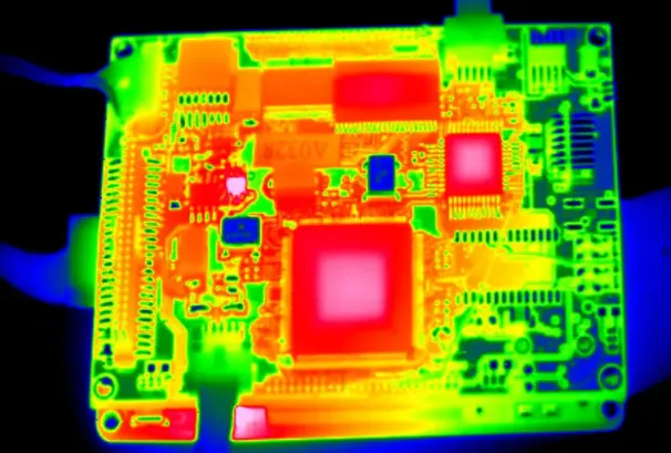
3. Thermal Management in PTH Design
Heat dissipation is a critical concern when dealing with high currents. PTHs can become hotspots if the heat generated by current flow isn’t managed effectively. Poor thermal management in PTH design can lead to delamination, cracking, or even complete failure of the board. Later in this post, we’ll explore specific strategies to address thermal issues and ensure reliable operation under high-current conditions.
Techniques for Increasing PTH Current Capacity
Now that we’ve covered the key factors influencing PTH current rating, let’s dive into actionable techniques for increasing PTH current capacity in your PCB designs. These methods are tailored for engineers looking to push the limits of high-current applications while maintaining reliability.
1. Optimize Copper Plating Thickness
As mentioned earlier, thicker copper plating inside the PTH reduces resistance and boosts current capacity. When specifying your PCB design, request heavier copper plating for PTHs, especially in power delivery areas. For instance, moving from a standard 1 oz/ft2 (35 micrometers) copper weight to 2 oz/ft2 (70 micrometers) or higher can make a substantial difference. Note that this applies not just to PTHs but also to the traces connected to them, as the entire current path must be optimized.
Additionally, ensure that the plating process achieves uniform coverage inside the holes. Poor plating can create thin spots or voids, which act as high-resistance points and potential failure areas. Work with your PCB manufacturer to confirm quality control measures for plating consistency.
2. Use Multiple PTHs for High-Current Paths
For applications requiring very high currents, a single PTH may not suffice, even with optimized plating. A practical solution is to use multiple PTHs in parallel for the same connection. This distributes the current across several holes, reducing the load on each one and minimizing heat buildup. For example, instead of routing 20 amps through a single PTH, you could use four PTHs, each handling 5 amps, to achieve the same result with lower thermal stress.
This technique also improves redundancy, as the failure of one PTH won’t necessarily disrupt the entire circuit. Just ensure that your layout allows for the additional space required for multiple holes.
3. Incorporate Thermal Vias for Heat Dissipation
Thermal vias are small, plated holes placed near high-current PTHs to help dissipate heat. While they don’t carry significant current themselves, they provide a path for heat to transfer from hot spots to other layers of the board or to a heat sink. For effective thermal management in PTH design, place thermal vias around power component mounting holes or high-current PTHs, connecting them to ground planes or other large copper areas that can spread heat.
A typical thermal via might have a diameter of 0.010 to 0.012 inches (0.25 to 0.3 mm), with several vias arranged in a grid pattern for maximum effect. Be cautious not to overcrowd the area, as this can weaken the board’s structural integrity.
4. Select Appropriate Materials for High-Current Designs
The base material of your PCB affects how well it handles high currents and heat. Standard FR-4 material is suitable for many applications, but for high-current designs, consider high-temperature laminates or materials with better thermal conductivity. These materials can withstand the elevated temperatures associated with high-current PTHs and prevent degradation over time.
Additionally, ensure that the solder used for through-hole components has a high melting point and good thermal stability. Poor solder joints can create high-resistance points, undermining the benefits of optimized PTH design.
Best Practices for High-Current PCB Design with PTH
Beyond specific techniques for increasing PTH current capacity, adopting best practices in your overall PCB design process can further enhance performance. These guidelines focus on creating reliable, efficient boards for high-current applications.
1. Design Wide Traces to Complement PTH Capacity
Even if your PTHs are optimized for high current, the traces connected to them must also be capable of handling the load. Use wider traces to reduce resistance and prevent bottlenecks in the current path. As a rule of thumb, for every 10 amps of current, a trace width of at least 0.1 inches (2.54 mm) is recommended for 1 oz/ft2 copper at room temperature. Adjust this based on your copper weight and expected operating conditions.
Online calculators or design software can help you determine the exact trace width needed for your current requirements, ensuring that no part of the circuit becomes a weak link.
2. Minimize PTH Aspect Ratio
As discussed earlier, a high aspect ratio can lead to uneven copper plating and reduced current capacity. When possible, design your PCB with thinner boards or larger hole diameters to keep the aspect ratio low. A ratio of 6:1 or lower is generally ideal for ensuring uniform plating and reliable performance in high-current PTHs.
3. Perform Thermal Simulations
Before finalizing your design, use simulation tools to model the thermal behavior of your PCB under high-current conditions. These tools can predict temperature rises around PTHs and identify potential hotspots. By addressing thermal issues during the design phase, you can avoid costly revisions or field failures. Aim for a maximum temperature rise of 10-20°C above ambient in critical areas to ensure long-term reliability.
4. Test and Validate Your Design
Once your PCB is manufactured, conduct thorough testing to validate the current carrying capacity of your PTHs. Use current stress tests to measure temperature rises and ensure they stay within acceptable limits. For instance, a temperature rise of more than 30°C under full load might indicate a need for design adjustments, such as thicker plating or additional thermal vias.
Testing also helps verify the mechanical integrity of PTHs, especially if they’re used for mounting heavy components or connectors that experience physical stress.
Common Challenges and How to Overcome Them
Designing PTHs for high-current applications isn’t without challenges. Here are a few common issues and practical solutions to address them.
1. Overheating Due to Insufficient Heat Dissipation
If thermal management in PTH design is inadequate, overheating can occur, leading to performance degradation or failure. To combat this, integrate thermal vias, use larger copper planes for heat spreading, and consider forced air cooling or heat sinks if the application allows. Monitoring operating temperatures during testing can help you fine-tune these solutions.
2. Manufacturing Limitations on Copper Thickness
Some manufacturers may have limits on how thick they can plate copper inside PTHs, especially for small-diameter holes. If you’re unable to achieve the desired thickness, consider increasing the number of PTHs or using larger holes to compensate. Clear communication with your manufacturer during the design phase can help align expectations and avoid surprises.
3. Space Constraints in Dense Layouts
In densely packed PCBs, finding room for multiple PTHs or thermal vias can be difficult. In such cases, prioritize critical high-current paths and use smaller thermal vias strategically placed around key areas. You might also explore multilayer designs to distribute current across more layers, reducing the load on individual PTHs.
Conclusion: Building Reliable High-Current PCB Designs
Maximizing the current carrying capacity of plated through-holes is a cornerstone of effective high-current PCB design. By focusing on factors like PTH copper plating thickness, hole diameter, and thermal management in PTH design, you can significantly enhance the performance and reliability of your boards. Techniques such as using thicker copper, incorporating multiple PTHs, and adding thermal vias provide practical ways to increase PTH current capacity, while best practices like wide traces and thermal simulations ensure a holistic approach to design.
Whether you’re designing for power supplies, motor controllers, or other demanding applications, these strategies will help you create PCBs that handle high currents with ease. Remember to validate your designs through testing and work closely with your manufacturing partner to achieve the best results. With the right techniques and attention to detail, your high-current PCB designs can meet even the most challenging requirements.


