 ALLPCB


In the world of printed circuit board (PCB) design, efficiency and precision are key. PCB stackup planning software is a powerful tool that helps engineers streamline the design process by simplifying complex tasks like impedance calculation, material selection, and simulation. If you're looking to optimize your workflow and ensure high-quality designs, using specialized planning tools for PCB stackup can save time and reduce errors. In this blog post, we'll dive deep into how these tools work, why they matter, and how you can use them to enhance your design automation process.
What Is PCB Stackup Planning Software and Why Does It Matter?
PCB stackup planning software is a digital solution designed to help engineers define the arrangement of layers in a PCB, including copper layers, dielectric materials, and other components. These tools are critical for modern designs, especially in high-speed and high-frequency applications where signal integrity and impedance control are non-negotiable. By using PCB stackup software, you can automate repetitive tasks, calculate critical parameters, and simulate performance before fabrication.
The importance of these tools lies in their ability to prevent costly mistakes. A poorly planned stackup can lead to signal interference, power delivery issues, or even complete design failure. With planning tools, you can ensure that your PCB meets performance standards while staying within budget and manufacturing constraints. Whether you're working on a simple two-layer board or a complex multilayer design, these tools are essential for success.
Key Features of PCB Stackup Planning Software
Before diving into how to use PCB stackup software, let's explore the core features that make these tools so valuable. Understanding these functionalities will help you choose the right tool and maximize its benefits for your projects.
1. Impedance Calculation
Impedance control is crucial for high-speed designs where signal integrity depends on maintaining consistent impedance across traces. PCB stackup software includes built-in calculators that analyze trace width, layer thickness, and dielectric properties to determine impedance values. For instance, achieving a standard 50-ohm impedance for a differential pair might require specific trace spacing and dielectric constants, which the software can compute instantly.
Without these tools, engineers would need to perform manual calculations or rely on separate field solvers, which can be time-consuming and prone to errors. With automated impedance calculation, you can test multiple configurations in minutes and ensure your design meets signal integrity requirements.
2. Material Selection Assistance
Choosing the right materials for your PCB stackup is vital for performance and cost. Different dielectric materials, such as FR-4 or high-frequency laminates, have unique properties like dielectric constant (Dk) and loss tangent (Df) that affect signal speed and loss. PCB stackup planning tools often include libraries of materials with detailed specifications, allowing you to compare options and select the best one for your design.
For example, if you're designing a board for a 5G application, you might need a material with a low Dk value (around 3.0) to minimize signal delay. The software can suggest suitable materials and show how they impact your stackup's overall performance.
3. Simulation Capabilities
Simulation is another powerful feature of PCB stackup software. These tools allow you to model how your design will behave under real-world conditions, identifying potential issues like crosstalk or power plane resonance before fabrication. By running simulations, you can tweak layer arrangements or materials to optimize performance without building physical prototypes.
Simulation also helps validate impedance calculations and signal integrity, ensuring that your design operates as intended at high frequencies, such as 10 GHz or above, where even small deviations can cause significant issues.
4. Design Automation
Automation is at the heart of modern PCB stackup tools. From generating stackup configurations to creating detailed documentation, these tools reduce manual effort and improve accuracy. Design automation features can produce drill plans, layer diagrams, and manufacturing files directly from your stackup design, streamlining communication with fabricators and minimizing the risk of misinterpretation.
Step-by-Step Guide to Using PCB Stackup Planning Software
Now that you understand the key features, let's walk through the process of using PCB stackup planning software to design a board. These steps are generalized to apply to most tools, ensuring you can adapt them to your specific platform.
Step 1: Define Your Design Requirements
Start by outlining the requirements for your PCB. Consider factors like the number of layers, signal speed, operating frequency, and power needs. For example, a high-speed design operating at 2.5 GHz might require at least four layers to separate signal and ground planes effectively. Having a clear set of goals will guide your stackup planning and help the software generate relevant suggestions.
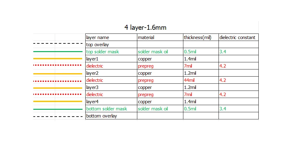
Input these parameters into the software, specifying constraints like board thickness (e.g., 1.6 mm for standard designs) or specific impedance targets (e.g., 100 ohms for differential pairs). This step sets the foundation for the rest of the design process.
Step 2: Build the Initial Stackup
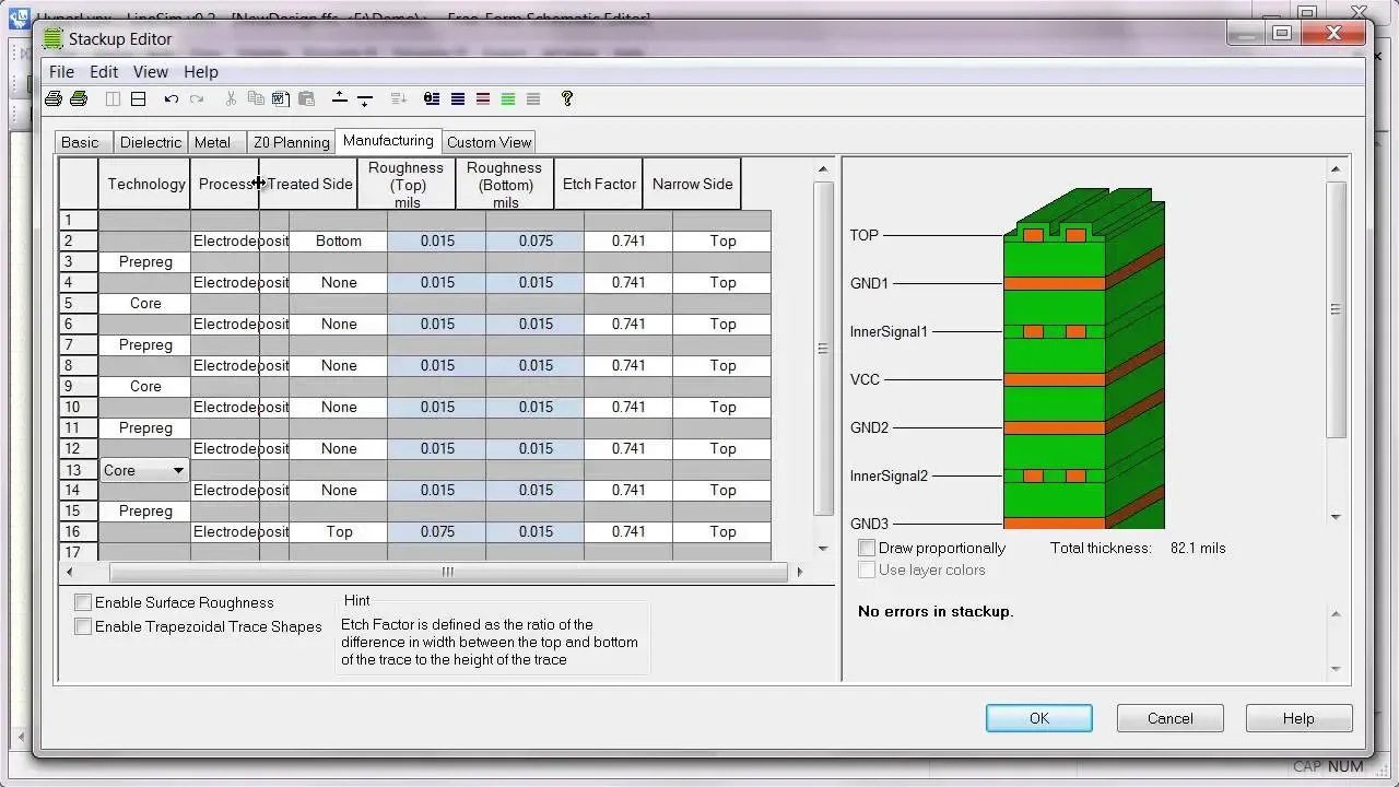
Use the software to create a preliminary stackup by selecting the number of layers and their types (signal, ground, power). Most tools offer templates for common configurations, such as a 6-layer stackup with alternating signal and ground layers to minimize crosstalk. Adjust the layer thickness and material properties based on your requirements.
At this stage, the software will often provide feedback on potential issues, such as unbalanced stackups that could lead to warpage during manufacturing. Make adjustments as needed to ensure symmetry and manufacturability.
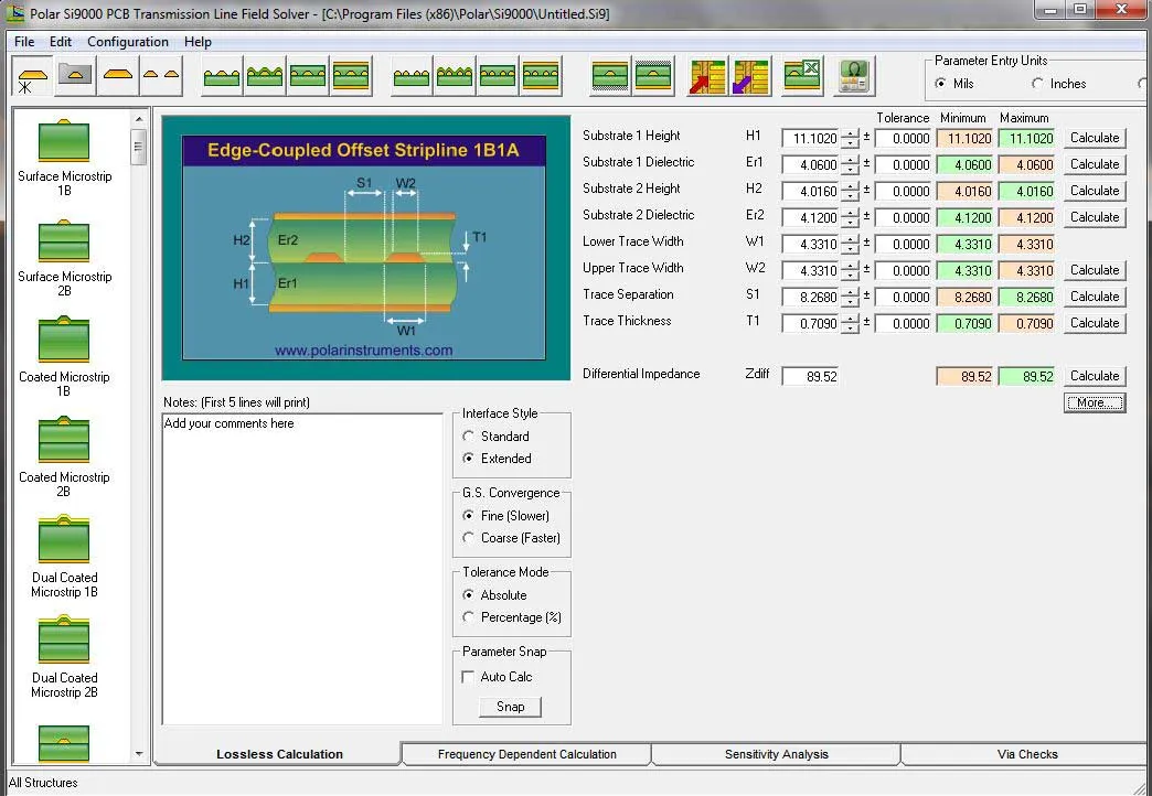
Step 3: Perform Impedance Calculations
With the initial stackup in place, use the impedance calculation feature to analyze critical traces. Input parameters like trace width (e.g., 5 mils for a 50-ohm line) and spacing for differential pairs. The software will calculate the impedance and suggest adjustments if the values fall outside your target range.
For instance, if the calculated impedance for a trace is 55 ohms instead of the desired 50 ohms, the tool might recommend increasing the dielectric thickness or reducing the trace width. This iterative process ensures precision in high-speed designs.
Step 4: Select Materials
Navigate to the material selection module in the software to choose appropriate dielectrics and copper weights for each layer. Look for materials that match your performance needs and budget. For a high-frequency design, you might opt for a material with a dielectric constant of 3.5 and a loss tangent of 0.002 to minimize signal loss.
The software will update the stackup model with the selected materials, recalculating impedance and other parameters to reflect the changes. This integration saves time and ensures consistency across your design.
Step 5: Run Simulations
Once your stackup is configured, use the simulation feature to test its performance. Simulate signal integrity to check for issues like reflections or crosstalk, especially if your design includes high-speed signals above 1 GHz. The software will generate reports or visualizations showing potential problem areas, allowing you to make data-driven adjustments.
For example, if the simulation reveals excessive crosstalk between adjacent signal layers, you might add a ground plane or increase spacing between traces. These insights are invaluable for avoiding costly redesigns.
Step 6: Finalize and Export for Manufacturing
After validating your stackup through simulation, finalize the design by generating documentation and manufacturing files. Most PCB stackup software can export detailed layer diagrams, drill plans, and impedance reports that fabricators need to build your board accurately. Review these files to ensure all specifications are correct before submission.
This step often includes design rule checks (DRC) within the software to catch any last-minute errors, such as layer misalignment or unsupported materials, ensuring a smooth transition to production.
Benefits of Using PCB Stackup Planning Tools
Integrating PCB stackup planning tools into your workflow offers several advantages that go beyond just simplifying the design process. Here are some key benefits that highlight their value for engineers.
Time and Cost Efficiency
Manual stackup planning can take hours or even days, especially for complex designs with multiple layers. Software automates these tasks, reducing design time by up to 50% in some cases. Additionally, by catching errors early through simulation, you avoid expensive rework or prototype failures, saving significant costs.
Improved Design Accuracy
Human error is a common issue in manual calculations, particularly for impedance and material compatibility. PCB stackup software minimizes these risks by providing precise calculations and real-time feedback, ensuring your design meets performance standards.
Enhanced Collaboration
Many tools allow you to share stackup designs and documentation with team members or fabricators directly through the platform. This seamless collaboration reduces miscommunication and ensures everyone is on the same page during the design and manufacturing process.
Best Practices for Maximizing PCB Stackup Software
To get the most out of PCB stackup planning tools, follow these best practices during your design process.
- Start with Clear Specifications: Always define your design goals upfront, including layer count, impedance targets, and frequency requirements, to guide the software's recommendations.
- Iterate and Simulate Often: Don’t settle for the first stackup configuration. Run multiple simulations with different setups to find the optimal balance of performance and cost.
- Stay Updated on Materials: Regularly check the software’s material library for new options, as advancements in PCB materials can offer better performance or lower costs.
- Document Everything: Use the software’s reporting features to create detailed documentation for every design iteration, ensuring transparency and traceability.
Conclusion: Transform Your Design Process with PCB Stackup Software
PCB stackup planning software is a game-changer for engineers looking to streamline their design process. From automating impedance calculations to assisting with material selection and running simulations, these tools offer a comprehensive solution for creating high-quality, reliable PCB designs. By following the steps outlined in this guide, you can harness the power of design automation to save time, reduce costs, and improve accuracy in your projects.
Whether you're tackling a simple board or a complex multilayer design, integrating PCB stackup planning tools into your workflow is a step toward smarter, more efficient engineering. Embrace these technologies to stay ahead in the fast-paced world of electronics design and ensure your boards meet the highest standards of performance and manufacturability.


