 ALLPCB


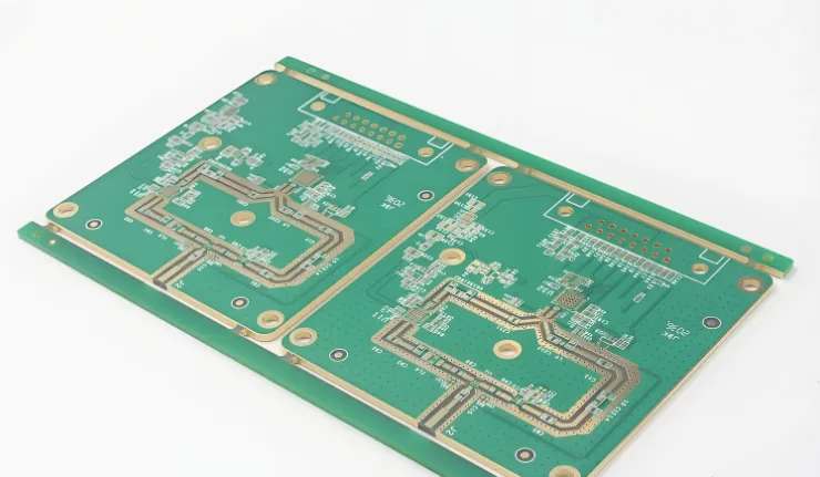
In the fast-paced world of algorithmic trading, every microsecond counts. High-speed PCB design plays a critical role in minimizing latency for trading systems, ensuring that data travels as quickly as possible between components. This blog dives deep into creating low latency PCB designs tailored for algorithmic trading, focusing on high-frequency PCB layout, signal integrity, impedance matching, and reducing signal reflections. Whether you're an engineer or a designer working on trading hardware, you'll find practical tips and detailed insights to optimize your PCB for speed and performance.
Why Low Latency PCB Design Matters in Algorithmic Trading
Algorithmic trading systems rely on split-second decisions to execute trades, often processing massive amounts of data in real time. Latency—the time it takes for a signal to travel through the system—can make or break profitability. A delay of just 1 microsecond can result in missed opportunities or significant financial losses in high-frequency trading environments. This is where low latency PCB design becomes essential. By optimizing the layout and components of a printed circuit board (PCB), engineers can reduce signal delays and ensure faster communication between processors, memory, and network interfaces.
In this post, we’ll explore the key principles of high-speed PCB design for trading systems, breaking down complex concepts into actionable steps. Let’s start with the foundation: understanding high-frequency signals and their impact on PCB performance.
Understanding High-Frequency PCB Layout for Trading Systems
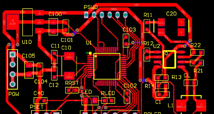
High-frequency PCB layout is the art of designing boards to handle signals that switch at extremely fast rates, often in the gigahertz range. In algorithmic trading systems, these signals carry critical data between components like field-programmable gate arrays (FPGAs), central processing units (CPUs), and high-speed network interfaces. A poorly designed layout can introduce delays, noise, or signal loss, all of which increase latency.
To create an effective high-frequency PCB layout, focus on the following principles:
- Minimize Trace Lengths: Shorter traces reduce the time it takes for a signal to travel from one point to another. For example, a signal traveling through a 1-inch trace on a standard FR-4 material takes approximately 150 picoseconds. Cutting trace lengths even by a few millimeters can shave off critical time in trading systems.
- Avoid Sharp Bends: Sharp angles in traces can cause signal reflections and electromagnetic interference (EMI). Use 45-degree angles or smooth curves instead of 90-degree turns to maintain signal quality.
- Use Differential Pairs: High-speed signals, such as those in Ethernet or PCIe interfaces, often use differential pairs to reduce noise. Keep these pairs close together and match their lengths to within 5 mils (0.005 inches) to prevent timing mismatches.
By applying these layout techniques, you can significantly lower latency and ensure that your PCB handles high-frequency signals efficiently.
Signal Integrity in Trading PCBs: The Backbone of Performance
Signal integrity refers to the quality of an electrical signal as it travels through a PCB. In trading systems, maintaining signal integrity in trading PCBs is non-negotiable because any distortion or noise can lead to data errors and slower processing times. Poor signal integrity can result from issues like crosstalk, signal reflections, or improper grounding.
Here are key strategies to ensure signal integrity:
- Proper Ground Planes: A solid ground plane beneath signal traces reduces noise and provides a return path for high-frequency signals. Avoid splitting ground planes, as this can create unwanted impedance changes.
- Control Crosstalk: Crosstalk happens when signals from adjacent traces interfere with each other. To minimize this, maintain a spacing of at least 3 times the trace width (known as the 3W rule) between high-speed traces.
- Termination Techniques: Use termination resistors to match the impedance of the trace to the load, reducing reflections. For instance, a 50-ohm termination resistor is common for high-speed signals like those in USB 3.0 or Ethernet lines used in trading hardware.
Signal integrity directly impacts latency. A clean, undistorted signal travels faster and requires less error correction, keeping your trading system responsive.
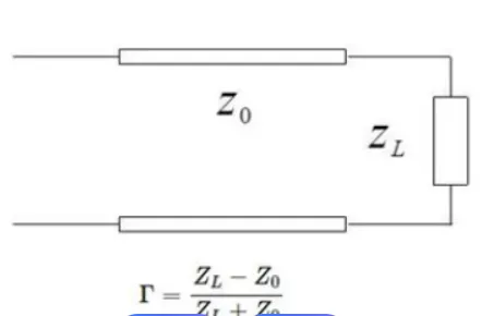
Impedance Matching for High-Speed PCBs: Eliminating Delays
Impedance matching for high-speed PCBs is a critical step in minimizing latency. Impedance is the resistance a signal encounters as it travels through a trace, and mismatches can cause reflections that delay or distort the signal. In algorithmic trading systems, where signals must travel at speeds exceeding 5 Gbps, even small impedance mismatches can add microseconds of delay.
To achieve proper impedance matching, consider these tips:
- Calculate Trace Impedance: Use tools or formulas to design traces with a specific impedance, typically 50 ohms for single-ended signals or 100 ohms for differential pairs. Factors like trace width, thickness, and the dielectric constant of the PCB material (e.g., FR-4 with a dielectric constant of 4.2) affect impedance.
- Match Components: Ensure that the impedance of traces matches the input and output impedance of connected components, such as transceivers or FPGAs. A mismatch between a 50-ohm trace and a 75-ohm component can cause up to 33% of the signal to reflect back.
- Use Controlled Dielectric Materials: High-speed designs often require materials with consistent dielectric properties to maintain uniform impedance across the board.
By focusing on impedance matching, you can eliminate unnecessary signal reflections and ensure that data moves through the PCB with minimal delay.
Reducing Signal Reflections in PCBs for Faster Trading Systems
Signal reflections occur when a signal encounters a change in impedance along its path, causing part of the signal to bounce back. These reflections create noise and delay the effective transmission of data, which is disastrous for algorithmic trading systems that rely on split-second timing. Reducing signal reflections in PCBs is therefore a top priority for low latency design.
Here’s how to tackle signal reflections:
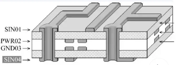
- Avoid Impedance Discontinuities: Sudden changes in trace width or layer transitions can cause reflections. Keep trace widths consistent and use vias sparingly, as they introduce impedance changes. If vias are necessary, back-drill them to remove unused stub lengths.
- Proper Termination: As mentioned earlier, termination resistors or other techniques like series or parallel termination can absorb reflected signals. For a high-speed signal at 10 Gbps, a mismatched termination can cause a reflection delay of over 100 picoseconds.
- Optimize Layer Stackup: Design your PCB stackup to minimize transitions between layers for high-speed signals. Keep critical traces on outer layers if possible, as inner layers can introduce more parasitic capacitance and inductance.
By reducing signal reflections, you ensure that data packets arrive at their destination without unnecessary delays, keeping your trading system competitive.
Material Selection for High-Speed PCB Design in Trading Systems
The choice of materials in a PCB directly affects signal speed and latency. Standard materials like FR-4 are cost-effective but may not support the ultra-high frequencies needed for algorithmic trading systems. At frequencies above 5 GHz, signal loss in FR-4 becomes significant, with a loss tangent of around 0.02 leading to attenuation of signals over long traces.
For high-speed designs, consider these alternatives:
- Low-Loss Materials: Materials like Rogers RO4003C or Isola IS680 offer lower dielectric constants (around 3.4) and loss tangents (as low as 0.0027), reducing signal loss and improving speed.
- Thin Dielectrics: Thinner dielectric layers between traces and ground planes reduce parasitic capacitance, allowing signals to travel faster.
- Copper Finish: Use smooth copper finishes to minimize skin effect losses at high frequencies, where current tends to flow on the surface of conductors.
Choosing the right materials can cut signal propagation delays by up to 20%, giving your trading system a competitive edge.
Advanced Techniques for Minimizing Latency in Trading PCBs
Beyond the basics, advanced techniques can further reduce latency in high-speed PCB designs for algorithmic trading. These methods require precision but deliver measurable results:
- Backplane Design: For systems with multiple boards, use high-speed backplanes with matched impedance connectors to maintain signal integrity across connections.
- Clock Distribution: Synchronize clocks across components to avoid timing jitter. Use low-skew clock buffers and keep clock traces as short as possible, ideally under 500 mils for 10 GHz signals.
- Simulation Tools: Before manufacturing, use simulation software to model signal behavior and identify potential latency issues. Tools can predict signal delays down to the picosecond, allowing for fine-tuned adjustments.
Implementing these advanced strategies ensures that every aspect of your PCB is optimized for speed, leaving no room for unnecessary delays.
Conclusion: Building the Fastest PCBs for Algorithmic Trading
High-speed PCB design for algorithmic trading systems is a complex but rewarding challenge. By focusing on low latency PCB design, high-frequency PCB layout, signal integrity in trading PCBs, impedance matching for high-speed PCBs, and reducing signal reflections in PCBs, you can create hardware that meets the demanding needs of modern trading environments. Every design decision—from trace length to material selection—impacts latency, and even small improvements can lead to significant gains in performance.
Start by applying the practical tips shared in this guide, such as minimizing trace lengths, ensuring proper impedance matching, and using low-loss materials. With careful planning and attention to detail, your PCB can become the foundation of a trading system that operates at lightning speed, giving you the edge in a competitive market.


