 ALLPCB


If you're designing a printed circuit board (PCB) using FR-4 material and wondering how to optimize via design for high-speed applications, you're in the right place. Proper via design on FR-4 PCBs is crucial for minimizing inductance and maximizing signal integrity, especially in high-speed circuits. In this comprehensive guide, we'll dive deep into techniques like managing FR-4 PCB via inductance, controlling via impedance FR-4, and using advanced methods such as blind via FR-4, buried via FR-4, via stitching FR-4, backdrilling FR-4, and high-speed via design FR-4. Let’s explore how to ensure your PCB performs at its best.
Why Via Design Matters in FR-4 PCBs
FR-4 is one of the most widely used materials for PCB fabrication due to its cost-effectiveness, durability, and good electrical properties. However, when it comes to high-speed designs, vias—those tiny holes that connect different layers of a PCB—can introduce challenges like inductance and impedance mismatches. These issues can degrade signal integrity, leading to data loss, crosstalk, or electromagnetic interference (EMI).
Vias act as pathways for signals to travel between layers, but if not designed properly, they can behave like small inductors or capacitors, disrupting the signal path. High inductance in vias slows down signal transitions, while poor impedance control causes reflections. For engineers working on high-speed circuits, optimizing FR-4 PCB via inductance and maintaining signal integrity is non-negotiable.
In this blog, we'll break down practical strategies to design vias on FR-4 PCBs, ensuring minimal inductance and maximum performance. Whether you're dealing with digital signals running at gigabit speeds or sensitive analog circuits, these tips will help you achieve reliable results.
Understanding FR-4 PCB Via Inductance
Inductance in vias is a key factor that affects signal performance on FR-4 PCBs. When a signal passes through a via, the structure creates a small loop of current, inducing inductance. This FR-4 PCB via inductance can cause delays in signal rise and fall times, which is especially problematic in high-speed designs operating at frequencies above 1 GHz.
The inductance of a via depends on its physical dimensions, such as diameter and length. A typical via on an FR-4 PCB might have an inductance of 0.5 to 1.5 nH (nanohenries), depending on its size and the surrounding layout. The longer and narrower the via, the higher the inductance. To minimize this, consider the following:
- Shorten Via Length: Use thinner PCB stackups or opt for blind or buried vias to reduce the via's vertical length.
- Increase Via Diameter: A larger diameter reduces inductance but be mindful of space constraints and manufacturing limits.
- Optimize Return Paths: Place ground planes close to signal layers to provide a low-inductance return path for signals transitioning through vias.
By focusing on these aspects, you can significantly lower FR-4 PCB via inductance and improve overall circuit performance.
Controlling Via Impedance in FR-4 Designs
Impedance mismatches are another common issue in high-speed PCB designs. When a signal travels through a via, any sudden change in impedance can cause reflections, leading to signal distortion. Maintaining consistent via impedance FR-4 is essential for preserving signal integrity.
In FR-4 materials, the dielectric constant (Dk) typically ranges from 4.2 to 4.5 at 1 MHz, which affects how signals propagate through the board. Vias often have a different impedance compared to the traces they connect due to their geometry and surrounding materials. For instance, a standard via might have an impedance of 50 ohms, but if the connected trace is designed for 50 ohms, mismatches can still occur due to parasitic effects.
To control via impedance FR-4, consider these techniques:
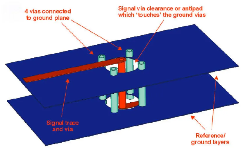
- Match Via Geometry to Trace Impedance: Use simulation tools to calculate the via dimensions that match the trace impedance. Adjusting the via pad size and antipad (the clearance around the via in the ground plane) can help.
- Use Ground Vias: Place ground vias near signal vias to stabilize impedance and reduce crosstalk.
- Avoid Unnecessary Via Stubs: Stubs (unused portions of a via) can act as antennas, causing reflections. Remove them through backdrilling or careful layer planning.
With proper attention to via impedance FR-4, you can minimize signal reflections and ensure smoother data transmission.
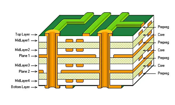
Advanced Via Types for FR-4 PCBs: Blind and Buried Vias
For complex, high-density designs, standard through-hole vias may not be the best choice. This is where advanced via types like blind via FR-4 and buried via FR-4 come into play. These vias offer benefits for both space efficiency and signal integrity.
Blind Vias in FR-4
A blind via FR-4 connects an outer layer of the PCB to an inner layer but does not go through the entire board. This reduces the via length, lowering inductance and minimizing signal delays. Blind vias are ideal for high-speed designs where signals only need to travel between specific layers.
For example, in a 6-layer FR-4 PCB, a blind via might connect layer 1 to layer 2, avoiding unnecessary stubs that could interfere with signals. However, blind vias can be more expensive to manufacture due to the precision required.
Buried Vias in FR-4
On the other hand, a buried via FR-4 connects two or more internal layers without reaching the outer surfaces. These are completely hidden within the board, saving surface space for components and traces. Buried vias also reduce inductance by shortening the signal path and are often used in high-density interconnect (HDI) designs on FR-4 PCBs.
Both blind and buried vias help in managing FR-4 PCB via inductance and improving signal integrity, but they require careful planning during the design phase to ensure manufacturability.
Via Stitching for Enhanced Grounding on FR-4 PCBs
Another powerful technique for maximizing signal integrity is via stitching FR-4. Via stitching involves placing multiple ground vias around signal vias or along the edges of ground planes to create a low-impedance return path for signals.
In high-speed designs, signals need a consistent return path to avoid EMI and crosstalk. Without proper grounding, signals passing through vias can induce noise in nearby traces. By using via stitching FR-4, you can ensure that the ground planes on different layers are tightly connected, reducing loop inductance and stabilizing impedance.
For instance, placing ground vias at intervals of 1/10th of the signal wavelength (e.g., 3 mm for a 10 GHz signal) around critical signal vias can significantly improve performance. This method is especially useful in FR-4 designs where cost constraints prevent the use of more advanced materials.
Backdrilling FR-4 PCBs to Eliminate Via Stubs
One of the most effective ways to address signal integrity issues in high-speed designs is through backdrilling FR-4. Backdrilling is a manufacturing process that removes unused portions of a via (known as stubs) after the PCB is fabricated.
Via stubs can act as resonant structures, causing signal reflections at specific frequencies. For example, a stub length of 0.5 mm on an FR-4 PCB can resonate at around 15 GHz, severely impacting signal quality. By using backdrilling FR-4, you can eliminate these stubs, ensuring cleaner signal transmission.
Backdrilling is particularly useful in multilayer FR-4 PCBs where signals only need to connect to intermediate layers. While it adds to manufacturing costs, the improvement in signal integrity for high-speed via design FR-4 often justifies the expense.
Best Practices for High-Speed Via Design on FR-4
Designing vias for high-speed applications on FR-4 PCBs requires a combination of good layout practices and an understanding of the material's limitations. Here are some best practices for high-speed via design FR-4 to ensure optimal performance:
- Minimize Via Count: Use fewer vias in the signal path to reduce inductance and impedance discontinuities. Route signals on the same layer whenever possible.
- Optimize Stackup: Design the PCB stackup to keep high-speed signals on outer layers or adjacent layers, reducing the need for long vias.
- Use Simulation Tools: Employ electromagnetic simulation software to model via behavior and predict issues like inductance and impedance mismatches before fabrication.
- Balance Cost and Performance: FR-4 is a cost-effective material, but it has higher dielectric losses compared to premium materials. For ultra-high-speed designs (above 10 GHz), consider hybrid stackups or alternative materials for critical layers.
By following these guidelines, you can achieve reliable high-speed via design FR-4 without compromising on signal integrity.
Common Challenges in FR-4 Via Design and How to Overcome Them
While FR-4 is a versatile and affordable material, it poses specific challenges for via design in high-speed applications. Let’s look at some common issues and their solutions:
- High Dielectric Loss: FR-4 has higher signal loss at frequencies above 5 GHz due to its dielectric properties. To mitigate this, keep trace and via lengths short and use ground planes effectively.
- Manufacturing Tolerances: Variations in via drilling and plating can affect impedance. Work closely with your fabrication partner to ensure tight tolerances, especially for blind and buried vias.
- Crosstalk: Vias placed too close to each other can cause crosstalk. Maintain adequate spacing (at least 3 times the via diameter) and use ground vias for shielding.
Addressing these challenges ensures that your FR-4 PCB design performs reliably, even in demanding applications.
Conclusion: Achieving Optimal Via Design on FR-4 PCBs
Designing vias on FR-4 PCBs for high-speed applications is a balancing act between cost, performance, and manufacturability. By focusing on minimizing FR-4 PCB via inductance, controlling via impedance FR-4, and leveraging techniques like blind via FR-4, buried via FR-4, via stitching FR-4, and backdrilling FR-4, you can significantly enhance signal integrity.
Whether you're working on a simple double-layer board or a complex multilayer design, the principles of high-speed via design FR-4 remain the same: keep vias short, match impedance, provide solid return paths, and eliminate stubs. With careful planning and the right tools, FR-4 can be an excellent choice for high-speed circuits without breaking the budget.
Armed with these strategies, you're ready to tackle via design challenges and build FR-4 PCBs that deliver top-notch performance. Start applying these techniques in your next project to see the difference in signal quality and reliability.


