ALLPCB


Are you a beginner diving into the world of PCB design and wondering, "What is an inner layer?" or "How do PCB layers work?" You're in the right place. Inner layers are critical components of multilayer printed circuit boards (PCBs), sandwiched between the outer layers to handle complex routing, power distribution, and signal integrity. In this guide, we’ll break down the basics of PCB design, focusing on inner layers, and provide actionable tips to help you design your first board with confidence.
Whether you're searching for "beginner PCB layers," "what is an inner layer," or "basic PCB design," this blog will walk you through the essentials. Let’s explore the structure, purpose, and best practices for working with inner layers to create efficient and reliable circuit boards.
What Are PCB Layers? A Quick Overview for Beginners
Before we dive into inner layers, let’s start with the basics of PCB layers. A printed circuit board is like a multi-layered sandwich, made up of conductive and insulating materials stacked together. The conductive layers are typically copper, used for routing electrical signals, while insulating layers (often made of a material like FR4, a type of fiberglass) separate them to prevent short circuits.
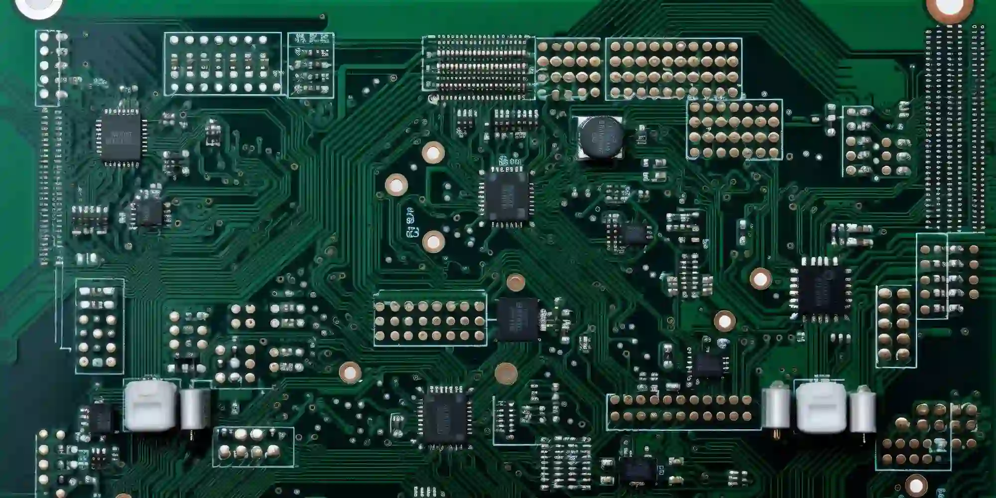
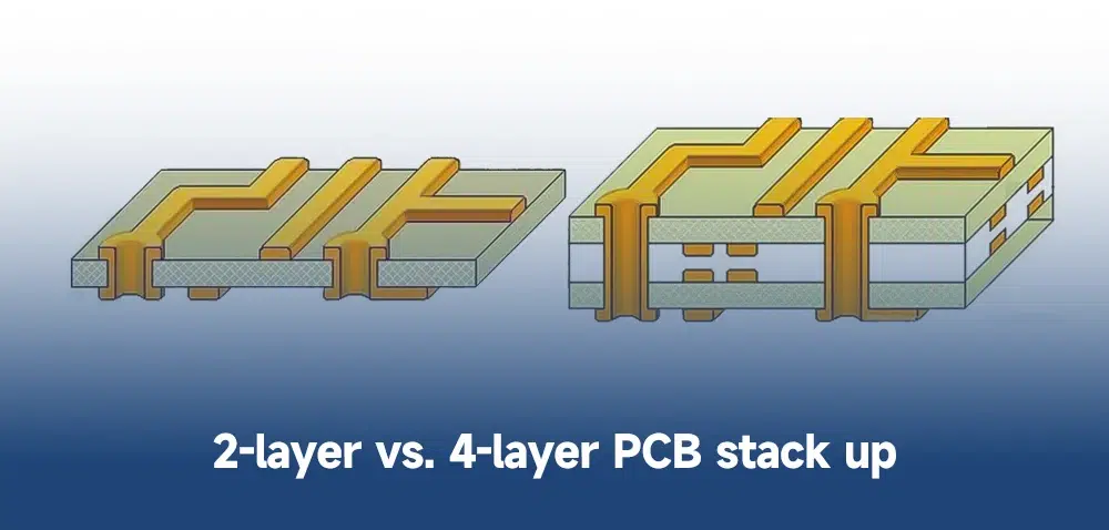
PCBs can be single-sided (one copper layer), double-sided (two copper layers), or multilayer (more than two layers). In multilayer boards, which are common in modern electronics, you’ll find outer layers (top and bottom) and inner layers (hidden inside the stack). These inner layers play a vital role in managing complex designs, especially for devices like smartphones, computers, and industrial equipment.
What Is an Inner Layer in PCB Design?
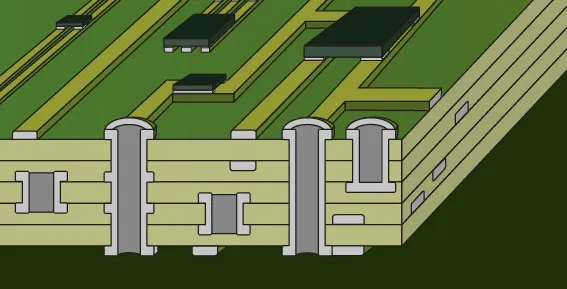
An inner layer is a copper layer located between the outer layers of a multilayer PCB. Unlike the top and bottom layers, which are exposed and often used for component placement and visible traces, inner layers are embedded within the board. They are laminated together with insulating material during manufacturing, making them invisible once the board is complete.
Inner layers are primarily used for routing signals, distributing power, and providing ground planes. For example, in a 4-layer PCB, you might have the top layer for components and signals, two inner layers for power and ground, and the bottom layer for additional routing. This setup helps reduce electromagnetic interference (EMI) and improves signal integrity by keeping critical traces short and shielded.
For beginners, understanding inner layers is crucial because they allow you to design more compact and efficient boards. Without them, you’d be limited to just the surface area of the outer layers, which can quickly become crowded in complex projects.
Why Are Inner Layers Important in Basic PCB Design?
Inner layers offer several benefits that make them essential for modern PCB designs. Here’s why they matter, especially for beginners tackling their first multilayer board:
- Space Efficiency: Inner layers provide extra room for traces, allowing you to fit more connections in a smaller footprint. This is critical for compact devices where space is limited.
- Improved Signal Integrity: By dedicating inner layers to ground or power planes, you create a stable reference for signals on adjacent layers. This reduces noise and crosstalk, which can degrade performance at high frequencies (e.g., above 100 MHz).
- Reduced EMI: Inner layers can act as shields, minimizing electromagnetic interference between signals or from external sources. For instance, placing a ground plane on an inner layer helps absorb unwanted noise.
- Thermal Management: Copper planes on inner layers can dissipate heat from high-power components, improving the board’s reliability over time.
For a beginner, starting with a 4-layer board (two outer and two inner layers) is a common choice for balancing complexity and functionality. It provides enough layers to separate power, ground, and signals while keeping the design manageable.
How Inner Layers Work in Multilayer PCBs
In a multilayer PCB, inner layers are stacked between insulating materials and bonded together under heat and pressure during manufacturing. Each layer is etched with copper traces or planes based on your design, just like the outer layers. However, since they’re internal, you can’t access them directly after the board is assembled.
To connect inner layers to other layers or components, designers use vias—small holes drilled through the board and plated with conductive material. For example, a through-hole via connects all layers, while a blind via connects an outer layer to an inner layer without going all the way through. These vias are essential for routing signals or power between layers.
A typical setup for a 4-layer board might look like this:
- Top Layer: Components and signal traces.
- Inner Layer 1: Ground plane to reduce noise.
- Inner Layer 2: Power plane to distribute voltage (e.g., 3.3V or 5V).
- Bottom Layer: Additional signal traces or secondary components.
This configuration ensures that power and ground are close to the signal layers, minimizing impedance and improving performance. For high-speed designs, like those involving USB or HDMI signals, keeping signal traces short and near a ground plane on an inner layer can reduce signal delay and distortion.
Steps to Design Inner Layers for Your First PCB
Designing inner layers might seem intimidating, but with the right approach, it’s manageable even for beginners. Here’s a step-by-step guide to help you get started with basic PCB design, focusing on inner layers:
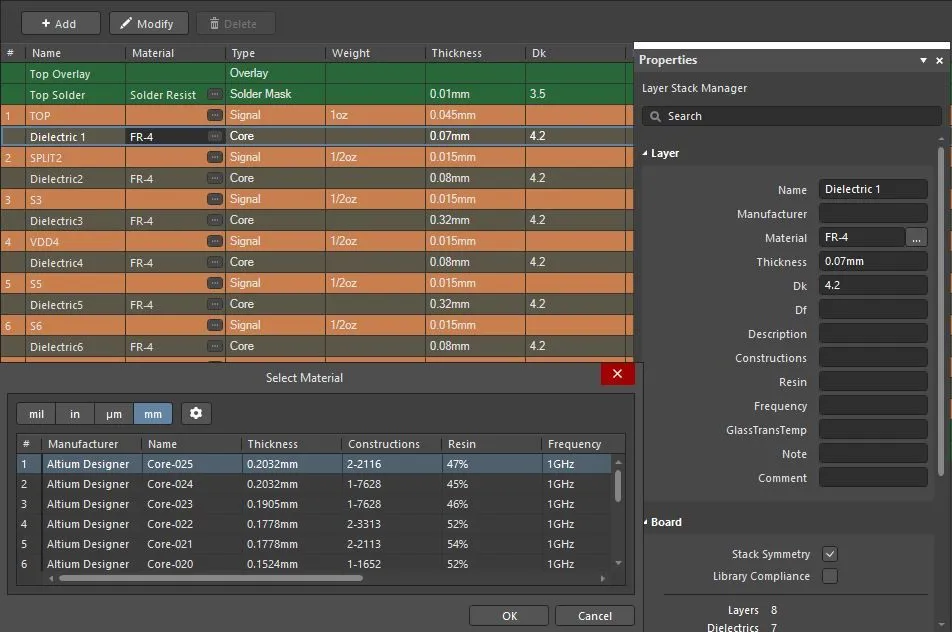
1. Plan Your Layer Stackup
Before you start routing, decide how many layers your board needs and what each layer will do. For a beginner, a 4-layer board is a good starting point. A common stackup is:
- Top: Signals and components
- Inner 1: Ground plane
- Inner 2: Power plane
- Bottom: Signals
This setup keeps power and ground planes close to signal layers, reducing loop inductance (often in the range of 1-10 nH) and improving performance.
2. Define Power and Ground Planes on Inner Layers
Dedicate inner layers to power and ground whenever possible. A solid ground plane on an inner layer provides a low-impedance path for return currents, which is critical for maintaining signal integrity. Similarly, a power plane ensures stable voltage distribution across the board, avoiding drops that could affect performance (e.g., a drop from 5V to 4.8V under load).
Use design software to create continuous copper pours for these planes, ensuring they cover as much area as possible without interruptions from traces or vias.
3. Route Signals with Inner Layers in Mind
While inner layers are often used for planes, you can also route signals on them if needed. Keep high-speed signals (e.g., clock signals at 50 MHz or higher) on inner layers adjacent to a ground plane to minimize interference. Avoid splitting planes unnecessarily, as gaps can disrupt return paths and increase EMI.
4. Use Vias Strategically
Connect inner layers to other layers using vias. For power and ground, place multiple vias near components to ensure low resistance (e.g., a via every 0.5 inches for high-current areas). For signals, minimize via usage to reduce inductance, which can slow down transitions (e.g., adding 1-2 ns delay per via in high-speed designs).
5. Check Design Rules and Constraints
Most design software includes design rule checks (DRC) to ensure your board meets manufacturing standards. For inner layers, pay attention to clearance (e.g., 0.2 mm between traces and vias) and copper thickness (often 1 oz/ft2 or 35 μm for standard designs). These rules prevent shorts and ensure reliability.
Common Mistakes to Avoid with Inner Layers
As a beginner, it’s easy to make mistakes when working with inner layers. Here are some pitfalls to watch out for:
- Splitting Planes Too Much: Cutting up power or ground planes with traces or vias creates gaps that disrupt current flow, increasing noise. Keep planes as solid as possible.
- Ignoring Impedance Control: For high-speed signals, mismatched impedance (e.g., targeting 50 ohms but achieving 60 ohms due to layer spacing) can cause reflections. Use calculators or software tools to match trace width and layer thickness.
- Overusing Vias: Too many vias on inner layers can weaken the board and add parasitic effects. Use them only where necessary.
- Forgetting Thermal Relief: When connecting vias to power or ground planes, add thermal relief pads (small gaps in copper) to make soldering easier during assembly.
Tips for Beginners Working on PCB Layers
Designing with inner layers doesn’t have to be overwhelming. Here are some practical tips to simplify the process:
- Start Small: Begin with a 4-layer design to learn the basics before moving to 6 or 8 layers.
- Use Reference Designs: Look at open-source projects or datasheets for layer stackup ideas. Many microcontroller boards provide sample layouts with inner layer configurations.
- Leverage Software Tools: Modern design tools offer simulation features to check signal integrity and EMI before manufacturing. Use them to spot issues early.
- Collaborate with Manufacturers: Share your design files with your PCB fabrication partner to confirm that inner layer specifications (e.g., dielectric thickness of 0.2 mm between layers) are achievable.
Conclusion: Mastering Inner Layers for Better PCB Designs
Understanding inner layers is a game-changer for anyone stepping into PCB design. These hidden copper layers allow you to create compact, efficient, and reliable boards by handling power, ground, and signals in a structured way. For beginners searching for "beginner PCB layers" or "basic PCB design," mastering inner layers is a key step toward designing professional-quality boards.
Start with a simple multilayer design, plan your stackup carefully, and use inner layers to manage power and ground effectively. By following the steps and tips in this guide, you’ll be well on your way to creating PCBs that perform reliably, even as a newcomer to the field. Remember, every great design begins with a solid foundation—and inner layers are a big part of that foundation.