 ALLPCB


Satellite payload PCBs must withstand the harsh conditions of space, including extreme temperatures ranging from -150°C to +150°C. Designing these boards requires careful material selection and layout strategies to ensure reliability and performance. In this comprehensive guide, we’ll explore how to choose the right materials like high-temperature PCB laminates and ceramic substrates for space, and apply layout techniques to manage thermal stress and CTE mismatch in satellite PCBs. Let’s dive into the critical aspects of designing PCBs for such demanding environments.
Why Extreme Temperatures Pose Challenges for Satellite Payload PCBs
Space is an unforgiving environment for electronics. Satellite payloads face rapid temperature swings as they orbit between direct sunlight and the cold vacuum of space. These fluctuations can cause thermal expansion, material degradation, and component failure if the PCB isn’t designed properly. For instance, a temperature shift of 100°C can induce significant stress on solder joints and traces if materials with mismatched coefficients of thermal expansion (CTE) are used.
Beyond temperature, factors like radiation and vacuum conditions add complexity. However, thermal management remains a primary concern because it directly impacts the structural integrity and electrical performance of the PCB. This is why selecting materials with high thermal stability, such as polyimide PCB for aerospace applications, and employing smart layout techniques are non-negotiable for success.

Material Selection for High-Temperature PCB Laminates
Choosing the right material is the foundation of designing a PCB that can survive extreme temperatures. High-temperature PCB laminates are specifically engineered to handle thermal stress and maintain performance. Here are the key materials to consider:
Polyimide PCB for Aerospace Applications
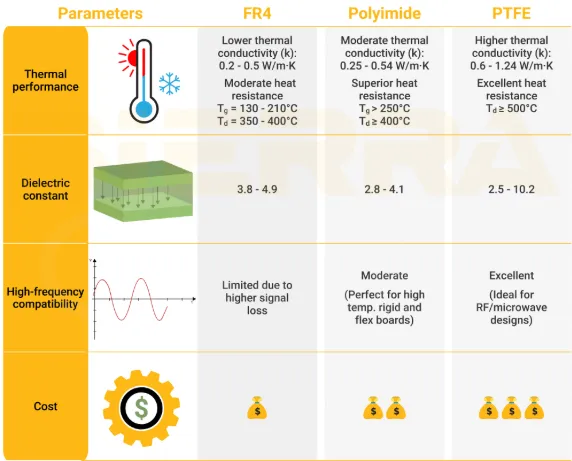
Polyimide is a top choice for satellite payload PCBs due to its excellent thermal stability. It can operate in temperatures ranging from -269°C to +400°C, making it ideal for aerospace environments. Additionally, polyimide offers high resistance to chemicals and radiation, which are common in space. Its flexibility also helps in applications where weight and space are limited, as it can be used in rigid-flex designs.
For example, a polyimide-based PCB might have a glass transition temperature (Tg) of over 250°C, ensuring it doesn’t soften or degrade during thermal cycles. This material is often paired with copper traces to balance conductivity and durability.
Ceramic Substrates for Space
Ceramic substrates for space applications are another excellent option for extreme environments. Materials like alumina (Al2O3) and aluminum nitride (AlN) provide superior thermal conductivity—up to 170 W/m·K for AlN—compared to traditional FR-4 laminates, which typically offer only 0.3 W/m·K. This high conductivity helps dissipate heat away from critical components, reducing the risk of overheating.
Ceramic substrates also have a low CTE, typically around 4-7 ppm/°C, which minimizes thermal stress when paired with components like silicon chips (CTE around 3 ppm/°C). Their rigidity and resistance to outgassing in vacuum conditions make them a reliable choice for satellite payloads.
Other High-Temperature PCB Laminates
Besides polyimide and ceramics, other high-temperature laminates like PTFE (polytetrafluoroethylene) and certain epoxy blends can be considered. PTFE offers a low dielectric constant (around 2.1) and can handle temperatures up to 260°C, making it suitable for high-frequency satellite communication circuits. However, it is softer and more expensive than polyimide, so it’s often reserved for specific use cases.
When selecting a laminate, always check the manufacturer’s datasheet for Tg, CTE, and thermal conductivity values to ensure compatibility with your design requirements. Balancing cost, performance, and availability is key.
Understanding CTE Mismatch in Satellite PCBs
One of the biggest challenges in designing satellite PCBs is managing CTE mismatch. The coefficient of thermal expansion (CTE) measures how much a material expands or contracts with temperature changes. A significant CTE mismatch between the PCB substrate, components, and solder joints can lead to mechanical stress, cracking, or delamination during thermal cycles.
For instance, a typical FR-4 substrate has a CTE of 14-17 ppm/°C, while a silicon chip might have a CTE of 3 ppm/°C. When subjected to a temperature swing of 100°C, the substrate expands much more than the chip, stressing the solder joints. In satellite applications, where repair is impossible, this mismatch can be catastrophic.
To mitigate CTE mismatch in satellite PCBs, consider these strategies:
- Use Low-CTE Materials: Opt for substrates like ceramics or specialized laminates with CTE values closer to those of the components (e.g., 4-7 ppm/°C).
- Underfill Components: Apply underfill materials around chips to distribute stress and protect solder joints during thermal expansion.
- Match Layer Stackup: Design the PCB stackup to balance CTE across layers, reducing warping or bending.
Thermal Stress Analysis for PCB Design
Thermal stress analysis for PCB design is a critical step in ensuring reliability under extreme temperatures. This process involves simulating how temperature changes affect the board’s materials and components. Advanced software tools can model thermal expansion, heat dissipation, and stress distribution to predict potential failure points.
For example, during thermal stress analysis, you might find that a specific solder joint experiences a shear stress of 50 MPa during a 100°C temperature swing. If this exceeds the material’s yield strength, redesigning the layout or changing materials becomes necessary. Key aspects of thermal stress analysis include:
- Finite Element Analysis (FEA): Use FEA to simulate thermal and mechanical stress on the PCB. This can help identify weak points in the design before manufacturing.
- Thermal Cycling Tests: Subject prototype boards to repeated temperature cycles (e.g., -55°C to +125°C) to observe real-world performance.
- Heat Dissipation Modeling: Ensure heat is evenly distributed across the board to avoid hotspots that could degrade components.
By incorporating thermal stress analysis early in the design phase, you can save time and resources by addressing issues before they become costly failures in space.
Layout Techniques for Thermal Management in Satellite PCBs
Beyond material selection, the layout of a satellite payload PCB plays a crucial role in managing extreme temperatures. A well-thought-out design can minimize thermal stress and enhance heat dissipation. Here are some proven layout techniques:
Optimize Component Placement
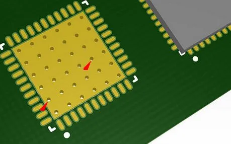
Place heat-generating components, such as power amplifiers or processors, away from temperature-sensitive parts. Position them near thermal vias or heat sinks to channel heat away efficiently. For instance, spacing components to allow a minimum of 0.5 mm clearance can improve airflow and reduce localized heating.
Use Thermal Vias and Copper Planes
Thermal vias are small holes filled with conductive material that transfer heat from one side of the PCB to the other. Placing an array of thermal vias under high-power components can reduce their operating temperature by up to 10-15°C. Additionally, large copper planes act as heat spreaders, distributing thermal energy across the board. Aim for copper thicknesses of 2 oz or higher for better conductivity.
Design for Symmetry
A symmetrical layout helps balance thermal expansion and contraction, reducing the risk of warping. For multilayer boards, ensure that copper distribution is even across layers to avoid uneven heating. This is especially important for satellite PCBs, where thermal gradients can cause mechanical failure.
Minimize Trace Lengths for High-Power Signals
Long traces carrying high current can generate excessive heat due to resistance. Keep these traces short and wide to reduce power loss and thermal buildup. For example, a trace width of 0.3 mm for a 1 A current can keep temperature rise below 10°C, based on standard IPC guidelines.
Additional Considerations for Satellite PCB Design
While thermal management is critical, other factors also influence the reliability of satellite payload PCBs in extreme temperatures. These include:
- Radiation Hardening: Use materials and components rated for high radiation levels to prevent degradation over time.
- Outgassing Prevention: Select materials with low outgassing properties to avoid contamination in the vacuum of space. Polyimide and ceramics typically excel in this area.
- Weight Optimization: Space missions prioritize lightweight designs. Balance thermal performance with material weight to meet mission requirements.
Conclusion: Building Reliable PCBs for Space Exploration
Designing satellite payload PCBs for extreme temperatures is a complex but achievable task with the right approach. By focusing on material selection—such as high-temperature PCB laminates like polyimide for aerospace and ceramic substrates for space—you can ensure thermal stability. Addressing CTE mismatch in satellite PCBs through careful material pairing and underfill techniques prevents mechanical failures. Additionally, thermal stress analysis for PCB design and strategic layout techniques, like thermal vias and symmetrical designs, enhance heat dissipation and reliability.
Every detail matters when a PCB operates in the unforgiving environment of space. Prioritizing these strategies during the design phase can mean the difference between mission success and failure. With the right materials and techniques, your satellite payload PCB will be ready to withstand the extreme temperature challenges of space exploration.


