 ALLPCB


When designing power PCBs, one of the most critical factors to consider is the current carrying capacity of the traces, especially in the inner layers. How much current can a trace handle without overheating or failing? The answer lies in understanding inner layer trace width, copper thickness, and industry standards like IPC-2221. In this comprehensive guide, we’ll explore how to calculate PCB current capacity, the role of copper thickness in power PCB design, and practical tips for optimizing your board for high-current applications.
Whether you’re an engineer working on high-power electronics or a designer looking to refine your skills, this blog will provide actionable insights into ensuring reliability and performance in your PCB designs. Let’s dive into the details of inner layer copper thickness and current carrying capacity.
Why Current Carrying Capacity Matters in Power PCBs
In power PCB design, the ability of traces to carry current without overheating is crucial. When current flows through a trace, it generates heat due to resistance. If the trace is too narrow or the copper too thin, the heat can build up, leading to performance issues, delamination, or even board failure. This is especially important in inner layers, where heat dissipation is more challenging compared to outer layers due to limited airflow and proximity to other heat sources within the board.
Current carrying capacity is influenced by several factors: trace width, copper thickness, ambient temperature, and whether the trace is on an inner or outer layer. By optimizing these elements, designers can ensure their PCBs handle the required power loads safely and efficiently. Standards like IPC-2221 and its successor IPC-2152 provide guidelines to calculate safe current limits and prevent thermal issues, which we’ll explore in detail.
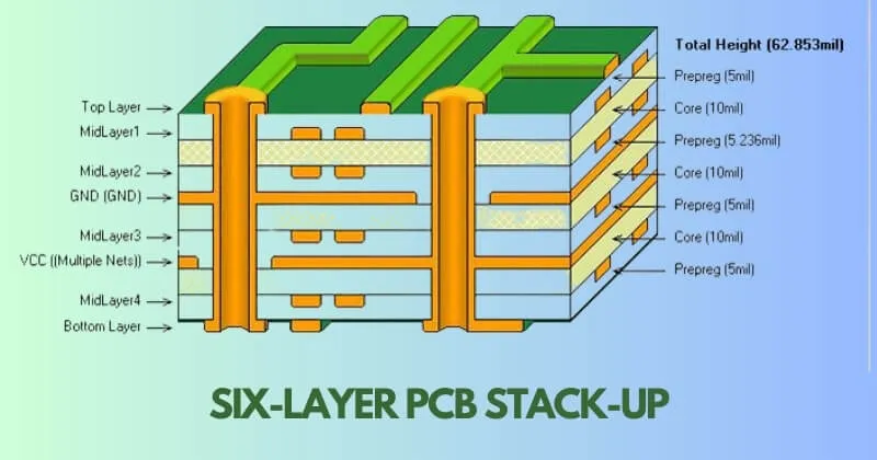
Understanding Inner Layer Challenges in Power PCB Design
Inner layers in multilayer PCBs present unique challenges for current carrying capacity. Unlike outer layers, which benefit from direct exposure to air for cooling, inner layers are sandwiched between other layers of material, trapping heat. This makes thermal management a priority when designing high-power boards with inner layer traces carrying significant current.
Additionally, inner layers often have less space for wider traces due to the complexity of routing in multilayer designs. Balancing trace width with available board real estate while ensuring sufficient copper thickness is a common hurdle. Designers must account for these constraints to avoid hotspots that could degrade components or cause long-term reliability issues.
What Is Copper Thickness and Why Does It Matter?
Copper thickness, often measured in ounces per square foot (oz/ft2), determines how much current a trace can carry. In PCB manufacturing, 1 oz/ft2 of copper equates to a thickness of about 1.4 mils (0.0014 inches or 35 micrometers). Common copper weights for power PCBs range from 1 oz to 3 oz or higher, with thicker copper used for higher current demands.
Thicker copper reduces the resistance of a trace, allowing it to carry more current without excessive heating. For inner layers, where heat dissipation is limited, increasing copper thickness is often a better solution than simply widening the trace, as space constraints may not allow for wider traces. However, thicker copper can increase manufacturing costs and may require adjustments in the PCB stack-up to maintain impedance control for signal integrity.
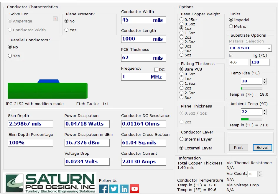
For example, a 1 oz copper trace with a width of 10 mils might safely carry 1 amp of current at a temperature rise of 10°C above ambient, based on IPC-2221 charts. Doubling the copper thickness to 2 oz can increase the current capacity to around 1.5-2 amps for the same temperature rise, depending on other factors like layer location and board material.
Calculating PCB Current Capacity: Trace Width and Copper Thickness
Determining the current carrying capacity of a PCB trace involves calculating the appropriate trace width and copper thickness for a given current load and acceptable temperature rise. The industry-standard guidelines for these calculations were historically provided by IPC-2221, but the updated IPC-2152 standard offers more accurate data based on extensive testing.
The general approach is to use a formula or chart to find the required trace width for a specific current, copper thickness, and temperature rise (commonly 10°C, 20°C, or 30°C above ambient). Here’s a simplified step-by-step process:
- Determine the Current Load: Identify the maximum current the trace needs to carry (e.g., 5 amps).
- Select Copper Thickness: Choose the copper weight for your design (e.g., 2 oz/ft2).
- Consider Temperature Rise: Decide on an acceptable temperature increase (e.g., 20°C) to avoid overheating.
- Account for Layer Location: Inner layers have lower current capacity than outer layers due to reduced heat dissipation. Use a derating factor (often around 50-60% of outer layer capacity) for inner traces.
- Use a Calculator or Chart: Refer to IPC-2152 charts or an online PCB trace width calculator to find the required width. For instance, a 2 oz inner layer trace carrying 5 amps with a 20°C rise might require a width of approximately 100 mils (0.1 inches).
These calculations ensure that the trace can handle the current without exceeding the temperature limits of the board material (typically FR-4, with a glass transition temperature of around 130-140°C). For power PCBs, it’s also critical to consider the thermal conductivity of the substrate and whether thermal vias or heat sinks are needed to manage heat in inner layers.
IPC-2221 and IPC-2152 Standards: Guidelines for Power PCB Design
The IPC-2221 standard has long been the go-to reference for PCB design, including current carrying capacity. It provides general guidelines for trace width and spacing based on current and voltage requirements. However, its data on current capacity was based on older testing from the 1950s and often resulted in conservative or overly optimistic estimates depending on the scenario.
The newer IPC-2152 standard, introduced as a more accurate replacement, is based on modern thermal testing and accounts for variables like board thickness, layer location, and the presence of planes or vias for heat dissipation. It provides detailed charts and equations to calculate trace width for a given current and temperature rise. For inner layers, IPC-2152 emphasizes derating the current capacity due to limited cooling, often recommending wider traces or thicker copper compared to outer layers.
For power PCB designers, adhering to these standards ensures reliability and safety. Ignoring them can lead to thermal runaway, where excessive heat damages the board or components over time. By following IPC-2152 guidelines, you can confidently design inner layer traces that handle high currents without risking failure.
Practical Tips for Optimizing Inner Layer Copper Thickness
Designing power PCBs with robust current carrying capacity in inner layers requires a combination of calculation, material selection, and layout optimization. Here are some practical tips to help you get started:
- Increase Copper Thickness: For high-current applications, specify 2 oz or 3 oz copper for inner layers instead of the standard 1 oz. This reduces resistance and heat generation, though it may raise costs.
- Use Wider Traces Where Possible: Even with thicker copper, wider traces distribute current more evenly and reduce hotspots. Balance this with space constraints in multilayer designs.
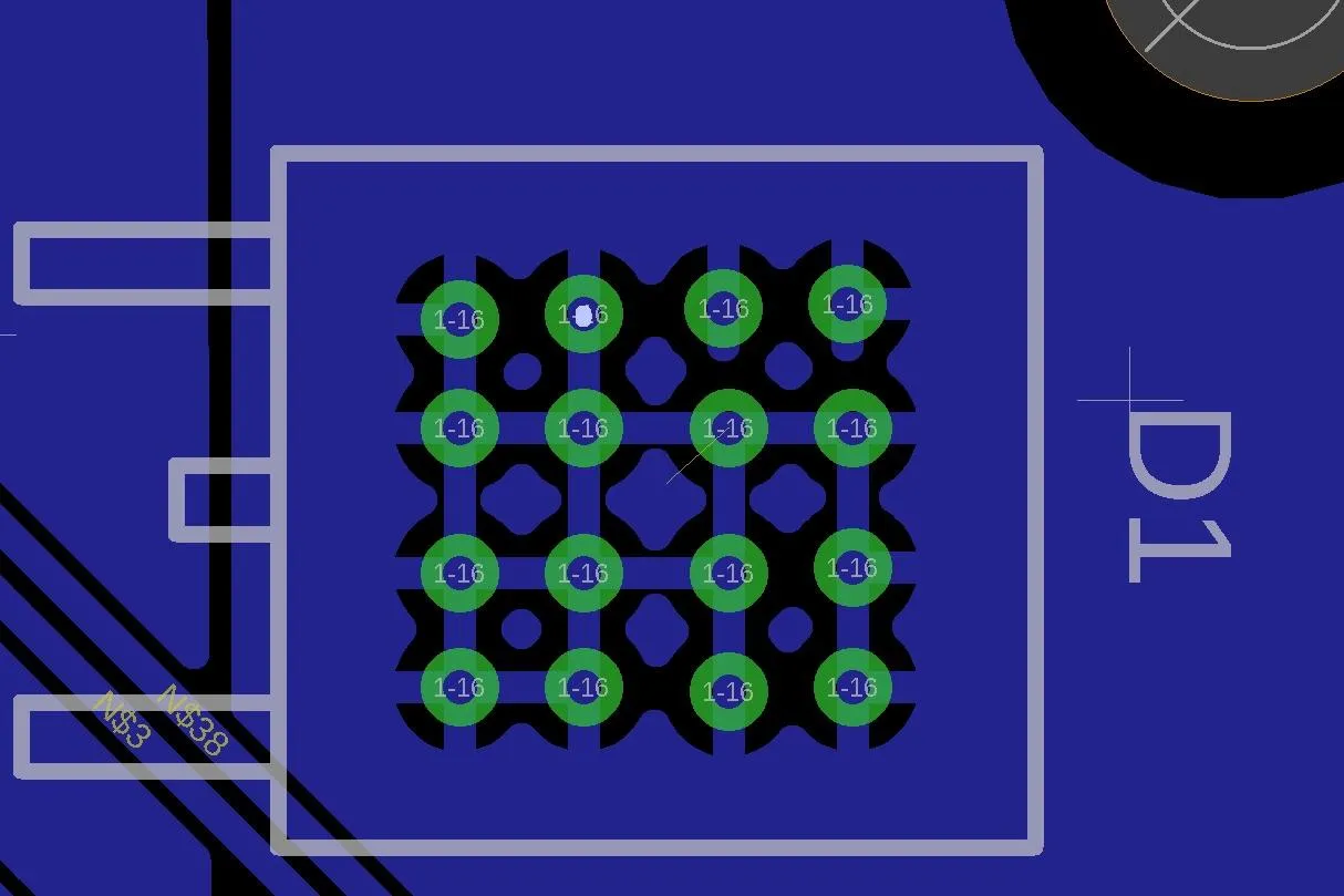
- Add Thermal Vias: Place thermal vias near high-current traces to transfer heat from inner layers to outer layers or heat sinks. For example, a grid of vias spaced 0.3 mm apart can significantly improve thermal performance.
- Choose High-Tg Materials: Use board materials with a higher glass transition temperature (Tg) for power applications. Standard FR-4 has a Tg of 130-140°C, but high-Tg variants (170-180°C) can handle more heat without degrading.
- Simulate Thermal Performance: Use PCB design software with thermal simulation tools to predict temperature rise in inner layers under load. Adjust trace widths and copper thickness based on simulation results.
- Plan for Derating: Always derate current capacity for inner layers by at least 50% compared to outer layers, as recommended by IPC-2152, to account for reduced cooling.
Common Mistakes to Avoid in Power PCB Design
Even experienced designers can make errors when dealing with current carrying capacity in inner layers. Here are some pitfalls to watch out for:
- Underestimating Heat Buildup: Failing to account for the limited cooling of inner layers can lead to overheating. Always use derating factors and verify with thermal simulations.
- Overlooking Voltage Drop: High-current traces can experience significant voltage drops over long distances due to resistance. Ensure trace width and copper thickness minimize this effect, especially in power delivery networks.
- Ignoring Manufacturing Limits: Specifying very thick copper (e.g., 4 oz or more) may not be feasible for all manufacturers or could impact layer stack-up and signal integrity. Check capabilities before finalizing your design.
- Neglecting Standards: Not following IPC-2221 or IPC-2152 guidelines can result in designs that fail under real-world conditions. Use these standards as a baseline for all power PCB projects.
Conclusion: Mastering Current Capacity in Power PCBs
Designing power PCBs with optimal current carrying capacity is a balancing act between trace width, copper thickness, thermal management, and adherence to industry standards like IPC-2221 and IPC-2152. Inner layers pose unique challenges due to limited heat dissipation, making careful calculation and design even more critical. By understanding how copper thickness impacts current capacity and applying practical tips like using thermal vias and high-Tg materials, you can create reliable, high-performance boards for demanding applications.


