 ALLPCB


When it comes to designing a printed circuit board (PCB) for your project, one of the first decisions you’ll face is choosing between a double-layer PCB and a multilayer PCB. So, which is best? In short, double-layer PCBs are ideal for simpler, cost-sensitive projects with basic functionality, while multilayer PCBs excel in complex, high-performance applications where space and signal integrity are critical. The right choice depends on your project’s needs, budget, and design complexity.
In this detailed guide, we’ll dive deep into the comparison of double-layer PCB vs multilayer PCB, exploring their differences, advantages, disadvantages, and costs. Whether you’re an engineer working on a prototype or a designer planning a high-tech device, this blog will help you make an informed decision for your next PCB design.
What Are Double-Layer PCBs and Multilayer PCBs?
Before we compare the two, let’s define what double-layer and multilayer PCBs are and how they’re structured.
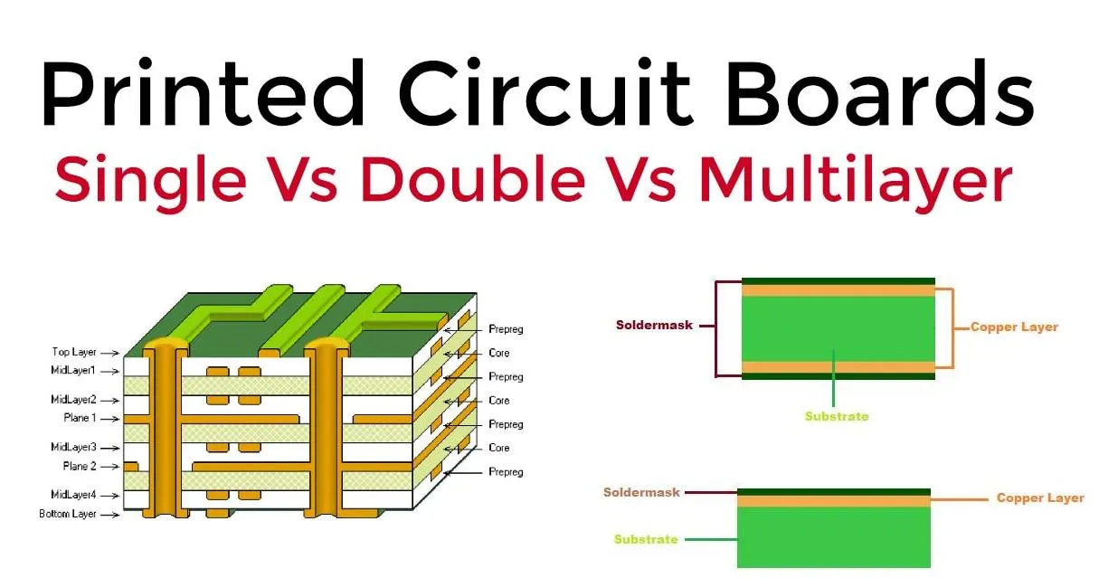
Double-Layer PCBs: Also known as 2-layer PCBs, these boards have conductive copper layers on both the top and bottom sides of a single insulating substrate. Vias (small holes) connect the two layers, allowing electrical signals to pass between them. These boards are commonly used in simpler electronics due to their straightforward design.
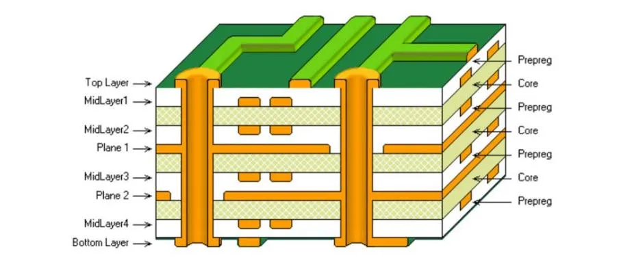
Multilayer PCBs: These boards consist of three or more conductive layers separated by insulating material. The layers are interconnected through vias, and the additional layers often include power and ground planes to improve performance. Multilayer PCBs are used in advanced electronics where higher circuit density and better signal integrity are required.
Key Differences in PCB Design: Double-Layer vs. Multilayer
Understanding the structural and functional differences between double-layer and multilayer PCBs is essential for making the right choice. Let’s break down the key aspects of PCB design comparison.
1. Number of Layers
The most obvious difference is the number of conductive layers. A double-layer PCB is limited to two layers, which restricts the complexity of the circuit. Multilayer PCBs, on the other hand, can have 4, 6, 8, or even more layers, providing more space for intricate designs and routing.
2. Circuit Density and Complexity
Double-layer PCBs are suitable for low to medium circuit density. They can handle basic circuits but may struggle with high-speed signals or dense component placement due to limited routing space. Multilayer PCBs support much higher circuit density, making them ideal for compact devices with numerous components, like smartphones or medical equipment.
3. Signal Integrity and Performance
In double-layer PCBs, signal integrity can be compromised due to longer trace lengths and potential crosstalk between signals. Multilayer PCBs often include dedicated ground and power planes, which reduce electromagnetic interference (EMI) and improve signal integrity. For instance, in high-speed designs, multilayer boards can maintain signal speeds above 1 GHz with minimal loss, while double-layer boards may struggle at such frequencies.
4. Size and Weight
Double-layer PCBs tend to be larger and heavier because all components and traces must fit on just two layers, often requiring more surface area. Multilayer PCBs allow for a smaller footprint by stacking layers vertically, reducing the overall size and weight of the board—a critical factor in portable devices.
Advantages and Disadvantages of Double-Layer PCBs
Let’s explore the pros and cons of double-layer PCBs to help you weigh their suitability for your project.
Advantages of Double-Layer PCBs
- Lower Cost: Double-layer PCBs are more affordable to manufacture compared to multilayer boards. The simpler design and fewer materials result in reduced production costs, often making them 30-50% cheaper than a 4-layer PCB for the same dimensions.
- Faster Production Time: With only two layers to fabricate and fewer steps in the manufacturing process, double-layer PCBs can be produced quickly, often within 3-5 days for standard orders.
- Easier Design and Debugging: Designing a 2-layer board is simpler, with fewer variables to consider. If issues arise, troubleshooting is easier since there are fewer layers to inspect.
- Suitable for Simple Applications: They work well for basic electronics like LED lighting, power supplies, and hobbyist projects where high performance isn’t a priority.
Disadvantages of Double-Layer PCBs
- Limited Complexity: These boards can’t handle complex circuits with many components or high-speed signals, making them unsuitable for advanced applications.
- Poor Signal Integrity: Without dedicated ground planes, double-layer PCBs are more prone to noise and EMI, which can degrade performance in sensitive designs.
- Larger Size: To accommodate all traces on just two layers, the board often needs a larger surface area, which isn’t ideal for compact devices.
Advantages and Disadvantages of Multilayer PCBs
Now, let’s look at the strengths and weaknesses of multilayer PCBs to see how they stack up.
Advantages of Multilayer PCBs
- Higher Circuit Density: With multiple layers, these boards can support more components and complex routing in a smaller space, perfect for modern electronics.
- Better Signal Integrity: Dedicated power and ground planes reduce impedance mismatches and EMI. For example, a 4-layer PCB can achieve impedance values as low as 50 ohms for controlled traces, ensuring stable high-speed signals.
- Compact and Lightweight: By stacking layers, multilayer PCBs save space, making them ideal for portable devices like wearables or IoT gadgets.
- Enhanced Durability: The additional layers and robust construction often make multilayer PCBs more resistant to physical stress and environmental factors.
Disadvantages of Multilayer PCBs
- Higher Cost: Manufacturing multilayer PCBs is more expensive due to the complexity of layering and the materials involved. A 4-layer PCB can cost 2-3 times more than a double-layer PCB of the same size.
- Longer Production Time: The intricate design and additional manufacturing steps mean longer lead times, often 7-14 days or more for standard production.
- Complex Design Process: Designing multilayer PCBs requires advanced software and expertise to manage layer stacking, via placement, and signal routing, increasing the risk of design errors.
PCB Cost Comparison: Double-Layer vs. Multilayer
Cost is often a deciding factor when choosing between double-layer and multilayer PCBs. Let’s break down the cost differences and what influences them.
Double-Layer PCB Cost: These boards are generally more budget-friendly. For a standard 100mm x 100mm board, the cost might range from $1 to $5 per unit for small to medium batch sizes (10-100 units). The price is lower because fewer materials and simpler processes are involved.
Multilayer PCB Cost: Multilayer boards are significantly more expensive due to the additional layers, complex manufacturing, and tighter tolerances. A 4-layer PCB of the same size might cost $5 to $15 per unit, while a 6-layer or 8-layer board can go up to $20 or more per unit. Costs also rise with advanced features like blind or buried vias.
Factors Affecting Cost: Beyond the number of layers, other factors like board size, material type (e.g., FR-4 vs. high-frequency laminates), surface finish (e.g., HASL vs. ENIG), and order quantity impact the final price. For high-volume production, the per-unit cost of both types decreases, but multilayer boards remain pricier overall.
Applications: When to Use Double-Layer vs. Multilayer PCBs
Choosing the right PCB type depends on the specific requirements of your application. Here’s a breakdown of where each type shines.
Double-Layer PCB Applications
- Simple Consumer Electronics: Devices like calculators, remote controls, and basic toys often use double-layer PCBs due to their low complexity and cost.
- Prototyping: For initial designs or proof-of-concept projects, double-layer boards are a cost-effective choice before moving to multilayer designs.
- Power Supplies: Basic power supply circuits with minimal components can work well on a 2-layer board.
Multilayer PCB Applications
- High-Tech Devices: Smartphones, tablets, and laptops rely on multilayer PCBs (often 6-12 layers) to pack complex circuitry into a small space.
- Industrial Equipment: Machinery control systems and automation devices use multilayer boards for reliable performance under demanding conditions.
- Medical Electronics: Devices like MRI machines and wearable health monitors require multilayer PCBs for precision and compact design.
- Telecommunications: High-speed networking equipment, such as routers and servers, depends on multilayer PCBs to manage fast data rates with minimal signal loss.
How to Decide: Double-Layer or Multilayer PCB?
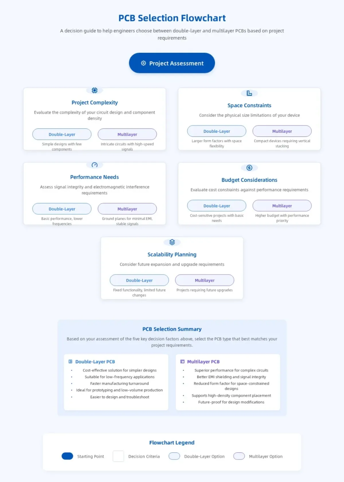
Selecting between a double-layer and multilayer PCB comes down to balancing several factors. Here’s a step-by-step approach to guide your decision.
- Evaluate Project Complexity: If your design involves only a few components and basic functionality, a double-layer PCB should suffice. For intricate circuits with high-speed signals or dense layouts, opt for a multilayer board.
- Consider Space Constraints: If your device needs to be compact, multilayer PCBs are the better choice due to their ability to stack layers vertically.
- Assess Performance Needs: For applications requiring minimal EMI and stable high-speed signals, multilayer PCBs with ground planes are essential.
- Set a Budget: If cost is a major concern and performance requirements are low, stick with a double-layer PCB to save on manufacturing expenses.
- Plan for Scalability: If you anticipate future upgrades or increased complexity, starting with a multilayer design might save redesign costs down the line.
Tips for Optimizing PCB Design Regardless of Layer Count
Whether you choose a double-layer or multilayer PCB, optimizing your design can enhance performance and reduce costs. Here are some practical tips.
- Plan Trace Routing Carefully: Minimize trace lengths to reduce signal delay and interference, especially on double-layer boards where space is limited.
- Use Proper Via Placement: Ensure vias are strategically placed to avoid signal congestion, particularly in multilayer designs with multiple connections.
- Select the Right Materials: Choose substrates and copper thicknesses based on your application’s thermal and electrical needs. For high-frequency designs, consider low-loss materials even for double-layer boards.
- Test and Iterate: Simulate your design using software tools to identify potential issues before manufacturing. This is especially critical for multilayer PCBs where errors are harder to fix.
- Work with Experienced Manufacturers: Partner with a reliable PCB fabrication service to ensure quality and adherence to design specifications, regardless of layer count.
Conclusion: Making the Right Choice for Your PCB Design
Deciding between a double-layer PCB and a multilayer PCB is a critical step in any electronics project. Double-layer PCBs offer affordability and simplicity, making them perfect for basic applications with minimal performance demands. Multilayer PCBs, while more expensive and complex, provide unmatched circuit density, signal integrity, and compactness for advanced, high-performance devices.
By carefully considering factors like project complexity, space limitations, performance requirements, and budget, you can confidently choose the PCB type that best fits your needs. Remember that the right design not only meets current requirements but also supports future scalability and reliability.
At ALLPCB, we’re committed to helping you bring your PCB designs to life with high-quality manufacturing and expert support. Whether you’re working on a simple 2-layer board or a sophisticated multilayer design, our services are tailored to ensure your project’s success.


