 ALLPCB


When it comes to designing a printed circuit board (PCB), every detail matters. One often overlooked aspect is the bottom layer silkscreen and whether it should be mirrored. So, why is mirroring crucial for the bottom layer silkscreen in PCB assembly? Simply put, mirroring ensures that text and markings on the bottom layer are readable and correctly oriented when viewed from the bottom side of the board during assembly and inspection. Without mirroring, labels can appear reversed, leading to confusion and potential errors in component placement or troubleshooting.
In this blog, we’ll dive deep into the importance of a mirrored silkscreen PCB bottom layer, explore how to handle a bottom silkscreen Gerber file, discuss reverse silkscreen printing techniques, and highlight how improper silkscreen handling can contribute to PCB assembly errors on the bottom layer. Whether you’re a seasoned engineer or new to PCB design, this guide will provide actionable insights to improve your design process and reduce costly mistakes.
What is PCB Silkscreen and Why Does It Matter?
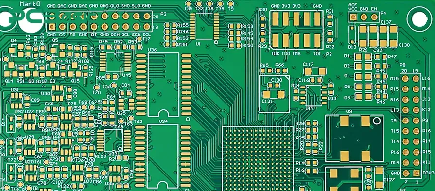
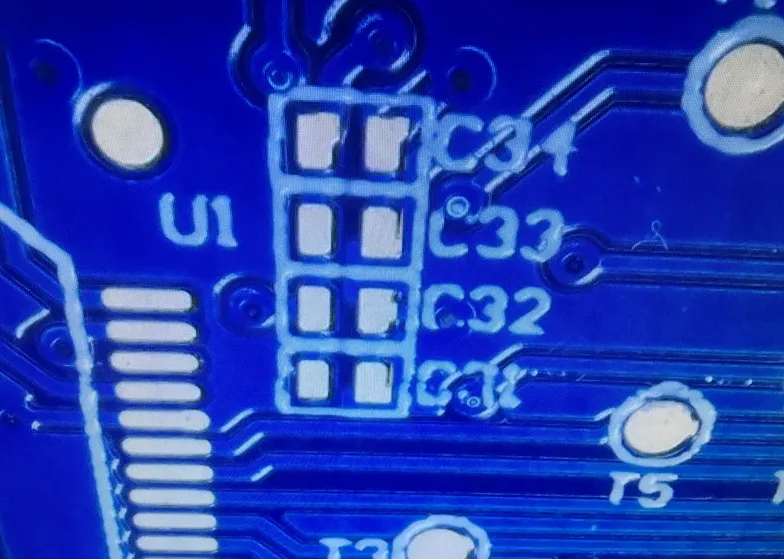
PCB silkscreen, often called the legend layer, is the non-conductive ink layer applied to the surface of a PCB. It includes text, symbols, and markings that provide essential information such as component designators, polarity indicators, and assembly instructions. This layer is typically applied to both the top and bottom sides of the board.
The silkscreen plays a vital role in the manufacturing and assembly process. It helps technicians identify where components go, ensures correct orientation, and simplifies troubleshooting during testing or repairs. Without clear and accurate silkscreen markings, the risk of errors increases significantly, especially on the bottom layer, where visibility and orientation can be trickier to manage.
Why Mirror the Bottom Layer Silkscreen?
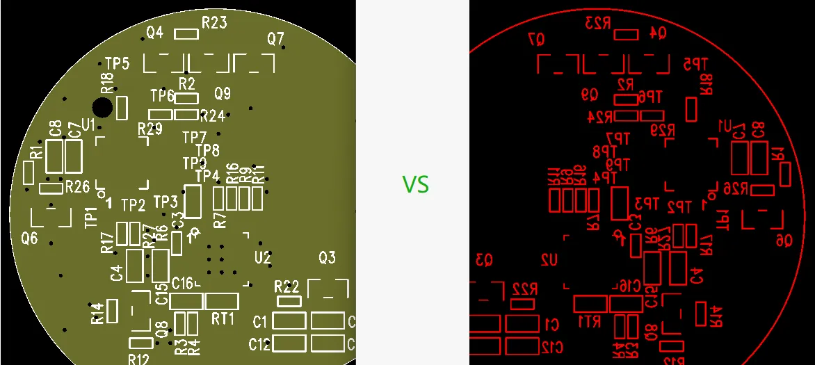
When designing a PCB, the bottom layer silkscreen must be mirrored to ensure readability. But why is this necessary? The answer lies in how we view and interact with the board during assembly and inspection.
On the top layer, silkscreen text is printed as it is designed because we view it directly from above. However, the bottom layer is viewed from the opposite side of the board. If the text on the bottom layer is not mirrored in the design phase, it will appear reversed when the board is flipped over for assembly or inspection. Imagine trying to read component labels or polarity markers that are backward—it’s a recipe for confusion.
Mirroring the mirrored silkscreen PCB bottom layer in your design software ensures that when the board is manufactured and viewed from the bottom, all text and symbols are oriented correctly. This small step can save hours of frustration and prevent costly mistakes during assembly.
How Mirroring Prevents PCB Assembly Errors on the Bottom Layer
Assembly errors are a common challenge in PCB manufacturing, and the bottom layer is particularly prone to mistakes if the silkscreen isn’t handled properly. Let’s explore how a correctly mirrored silkscreen can prevent PCB assembly errors on the bottom layer.
- Component Misplacement: Without clear, readable labels on the bottom layer, technicians may place components incorrectly. For example, a reversed polarity marker for a diode could lead to it being soldered backward, causing circuit failure. Mirroring ensures that all indicators are easy to interpret, reducing placement errors by up to 30% in some assembly scenarios.
- Orientation Issues: Many components, such as connectors or ICs, have specific pin orientations. If bottom layer markings are reversed, assemblers might misalign these components, leading to functional issues. A mirrored silkscreen provides clear guidance, ensuring proper orientation.
- Troubleshooting Challenges: During testing or repair, engineers often flip the board to inspect the bottom layer. If the silkscreen isn’t mirrored, identifying components or tracing connections becomes a tedious task, increasing the time and cost of debugging.
By prioritizing a mirrored bottom silkscreen, you can significantly reduce these risks and streamline the assembly process.
Handling the Bottom Silkscreen Gerber File: Best Practices
When preparing your PCB design for manufacturing, the bottom silkscreen Gerber file is a critical piece of the puzzle. Gerber files are the standard format used to communicate design data to manufacturers, and they include separate layers for the top and bottom silkscreen.
Here are some best practices to ensure your bottom silkscreen is correctly mirrored in the Gerber file:
- Mirror Only the Bottom Layer: In your PCB design software, ensure that only the bottom silkscreen layer is set to be mirrored. The top layer and other design elements, such as copper traces or solder mask, should remain unmirrored to avoid manufacturing errors.
- Double-Check Before Export: Before exporting your Gerber files, preview the bottom silkscreen layer to confirm that text and symbols appear reversed in the design view. This reversal ensures they will be readable on the physical board.
- Use Clear Layer Naming: Label your bottom silkscreen layer clearly (e.g., “Bottom Overlay” or “Bottom Silkscreen”) in the Gerber file to avoid confusion during manufacturing. This helps the fabricator identify which layer needs special handling.
- Communicate with Your Manufacturer: If you’re unsure whether your design software automatically mirrors the bottom layer, inform your manufacturer to double-check the silkscreen orientation. Clear communication can prevent costly reprints.
Following these steps ensures that your bottom silkscreen is correctly prepared, reducing the likelihood of errors during production.
Reverse Silkscreen Printing: Understanding the Process
The term reverse silkscreen printing often comes up when discussing bottom layer silkscreen. This refers to the process of designing the bottom silkscreen in a mirrored format so that it appears correctly when printed on the physical board. Let’s break down how this works.
In PCB manufacturing, the silkscreen is applied using a stencil or screen-printing process. The design data from your Gerber file dictates how the ink is laid out on the board. For the bottom layer, the manufacturer uses the mirrored design to ensure that text and symbols are oriented correctly when viewed from below. This “reverse” approach in the design phase results in a readable silkscreen on the finished product.
If the bottom layer silkscreen isn’t reversed during design, the manufacturer may need to manually adjust the data, which can introduce delays or errors. In some cases, boards may be produced with unreadable bottom markings, requiring a redesign and reprint—a process that can cost hundreds of dollars depending on the batch size.
To avoid these issues, always verify that your design software or Gerber export settings correctly handle reverse silkscreen printing for the bottom layer.
Common Mistakes with Bottom Layer Silkscreen and How to Avoid Them
Even experienced designers can make mistakes when handling the bottom layer silkscreen. Here are some common pitfalls and tips to avoid them:
- Forgetting to Mirror the Bottom Layer: This is the most frequent error. If the bottom silkscreen isn’t mirrored, all markings will appear backward on the physical board. Always double-check your design settings before exporting files.
- Overlapping Markings with Pads or Vias: Silkscreen ink should not cover solder pads or vias, as it can interfere with soldering. Ensure there’s a clearance of at least 0.2 mm between silkscreen markings and copper features on the bottom layer.
- Using Small or Unreadable Fonts: Tiny text or overly complex symbols can become illegible after printing, especially on the bottom layer where visibility might be limited. Use a minimum font size of 6 points (approximately 0.8 mm in height) for silkscreen text.
- Ignoring Manufacturer Guidelines: Different manufacturers may have specific requirements for silkscreen layers. Some may automatically mirror the bottom layer, while others expect you to do it. Always review their design rules before submission.
By paying attention to these details, you can avoid unnecessary delays and ensure a smooth assembly process.
The Impact of Bottom Layer Silkscreen on Manufacturing Costs
While the silkscreen layer might seem like a minor detail, errors in this area can have a significant impact on manufacturing costs. For instance, if a batch of 100 boards is produced with an unmirrored bottom silkscreen, the assembly team might spend an additional 2-3 hours correcting component placement issues. At an average labor rate of $50 per hour, this could add $150 or more to the project cost.
In worse cases, if the boards are unusable due to silkscreen errors, you may need to reorder the entire batch. For a small run of 100 boards at $5 per board, that’s a $500 loss, not including shipping and downtime. Investing a few extra minutes to verify the mirrored silkscreen PCB bottom layer during the design phase can save you from these expenses.
Tips for Designing an Effective Bottom Layer Silkscreen
Creating a well-designed bottom layer silkscreen goes beyond just mirroring the text. Here are some additional tips to enhance its effectiveness:
- Prioritize Essential Information: Only include critical markings on the bottom layer, such as component designators and polarity indicators. Avoid cluttering the space with unnecessary text.
- Ensure Contrast: Choose a silkscreen color that contrasts well with the board’s solder mask (e.g., white silkscreen on a green or blue mask). This improves readability, especially in low-light assembly environments.
- Test with a Prototype: Before ordering a full production run, create a prototype to verify that the bottom silkscreen is readable and correctly oriented. This can catch issues early and save costs.
- Use Standard Symbols: Stick to widely recognized symbols for polarity, grounding, and other indicators. Custom symbols might confuse assemblers unfamiliar with your design.
These practices will help ensure that your bottom layer silkscreen is both functional and user-friendly.
Conclusion: Mirror Your Bottom Silkscreen for Flawless PCB Assembly
The bottom layer silkscreen may seem like a small detail in the grand scheme of PCB design, but its impact on assembly accuracy and efficiency is undeniable. By mirroring the mirrored silkscreen PCB bottom layer, preparing a proper bottom silkscreen Gerber file, and understanding reverse silkscreen printing, you can prevent PCB assembly errors on the bottom layer and save time and money in the process.
At ALLPCB, we understand the importance of precision in every aspect of PCB design and manufacturing. By following the best practices outlined in this guide, you can ensure that your boards are assembled correctly the first time, every time. Take the extra step to verify your bottom layer silkscreen, and you’ll see the difference in the quality and reliability of your finished products.


