 ALLPCB


In the world of high-speed PCB design, signal integrity is everything. If you're dealing with high-frequency signals, even the smallest interference or loss can cause major performance issues. So, how can you ensure your PCB performs flawlessly at high speeds? The answer lies in a powerful technique called backdrilling. Backdrilling is a manufacturing process that removes unused portions of vias, known as via stubs, to minimize signal distortion and improve overall performance. In this blog, we'll dive deep into PCB backdrilling signal integrity, explore backdrilling benefits for high-speed designs, and explain its role in via stub removal, high-frequency PCB design, and impedance matching.
What Is Backdrilling and Why Does It Matter?
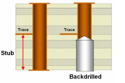
Backdrilling, also known as controlled depth drilling, is a specialized process used in PCB manufacturing. It involves drilling out the unused portion of a through-hole via after the initial plating process. This unused portion, called a via stub, can act like a tiny antenna, causing signal reflections and degrading performance in high-speed circuits. By removing the stub, backdrilling ensures cleaner signal transmission, making it a critical step for modern high-frequency PCB designs.
Why does this matter? In high-speed applications, such as data centers, telecommunications, and advanced computing, signals often operate at frequencies above 5 GHz. At these speeds, even a small via stub—sometimes just a few millimeters long—can introduce significant signal loss or crosstalk. Backdrilling eliminates this problem, acting as a superhero for maintaining signal integrity in demanding environments.
How Via Stubs Affect Signal Integrity in High-Speed PCBs
To understand the importance of backdrilling, let’s first look at via stubs and their impact on signal integrity. A via stub is the unused part of a through-hole via that extends beyond the signal layer it connects to. While this stub might seem harmless, it creates a resonant structure that reflects signals back along the trace. This reflection can lead to several issues:
- Signal Loss: At high frequencies, via stubs cause insertion loss, reducing the strength of the transmitted signal. For example, a stub as short as 0.5 mm can cause noticeable loss at 10 GHz.
- Signal Distortion: Reflections from the stub interfere with the main signal, leading to distortion and potential data errors.
- Crosstalk: Stub-induced reflections can couple with nearby traces, introducing unwanted noise in adjacent signals.
In high-speed designs, where timing and accuracy are critical, these effects can be catastrophic. For instance, in a 25 Gbps data transmission system, even a 1% signal loss can result in bit errors, slowing down or crashing the system. This is where via stub removal through backdrilling comes to the rescue, ensuring signals remain clean and reliable.
The Backdrilling Process: How It Works
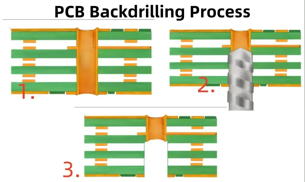
Backdrilling is a precise manufacturing technique that requires advanced equipment and expertise. Here's a step-by-step breakdown of how it works:
- Initial Via Drilling and Plating: The PCB is first drilled with through-hole vias, and the holes are plated with copper to create electrical connections between layers.
- Identification of Unused Stub: Designers identify which parts of the via are unused (i.e., the stub) based on the signal layer connections.
- Controlled Depth Drilling: Using a specialized drill, the unused portion of the via is removed from the opposite side of the board. The drill depth is carefully controlled to avoid damaging the active signal path.
- Inspection: The board undergoes inspection to ensure the stub has been removed without affecting the via’s integrity or nearby structures.
This process requires precision to avoid over-drilling, which could sever critical connections, or under-drilling, which might leave a residual stub. Modern manufacturing tools can achieve depth tolerances as tight as ±0.05 mm, ensuring reliable results even in complex multilayer boards.
Backdrilling Benefits for High-Speed PCB Designs
The advantages of backdrilling are numerous, especially when it comes to high-speed and high-frequency PCB design. Let’s explore the key backdrilling benefits for high-speed applications:
1. Improved Signal Integrity
By removing via stubs, backdrilling eliminates the primary source of signal reflections in through-hole vias. This results in cleaner waveforms and reduced jitter, which is essential for maintaining data accuracy at speeds above 10 Gbps. For example, studies have shown that backdrilling can reduce insertion loss by up to 0.5 dB at 20 GHz, a significant improvement for high-speed systems.
2. Reduced Crosstalk and EMI
Via stubs can radiate electromagnetic interference (EMI), affecting nearby traces and components. Backdrilling minimizes this radiation, reducing crosstalk between signals. This is especially important in dense PCB layouts where high-speed traces are closely packed.
3. Enhanced Impedance Matching
Impedance matching is critical in high-frequency PCB design to prevent signal reflections at connection points. Via stubs disrupt impedance continuity, creating mismatches that degrade performance. Backdrilling helps maintain consistent impedance—often targeting a standard value like 50 ohms—across the signal path, ensuring efficient energy transfer. Impedance matching with backdrilling can reduce return loss by as much as 10 dB in some designs.
4. Support for Higher Frequencies
As signal frequencies increase, the impact of via stubs becomes more pronounced. Backdrilling enables PCBs to handle frequencies beyond 20 GHz, making it a must-have for applications like 5G networks, advanced radar systems, and high-performance computing.
5. Cost-Effective Compared to Alternatives
While backdrilling adds a step to the manufacturing process, it is often more cost-effective than alternatives like blind or buried vias. These alternatives require additional lamination cycles and complex fabrication, driving up costs. Backdrilling, on the other hand, can be applied to standard through-hole designs with minimal added expense.
Applications of Backdrilling in High-Frequency PCB Design
Backdrilling is widely used in industries where high-frequency signals and fast data rates are the norm. Some common applications include:
- Telecommunications: Equipment for 4G and 5G networks relies on backdrilling to handle multi-gigabit data rates with minimal signal loss.
- Data Centers: Servers and networking hardware use backdrilling to support high-speed interconnects, such as PCIe 4.0 and 5.0, operating at 16 to 32 Gbps.
- Aerospace and Defense: Radar and communication systems in this sector often operate at frequencies above 10 GHz, where backdrilling is essential for reliable performance.
- Medical Devices: High-speed imaging and diagnostic equipment require clean signals for accurate data processing, making backdrilling a valuable technique.
In each of these fields, the ability to maintain signal integrity through via stub removal directly translates to better system performance and reliability.
Challenges and Considerations in Backdrilling
While backdrilling offers significant benefits, it’s not without challenges. Designers and manufacturers must consider the following factors:
- Precision Requirements: Backdrilling demands high accuracy to avoid damaging functional parts of the via. Even a slight error in drill depth can compromise the board’s performance.
- Increased Manufacturing Time: Adding a backdrilling step extends the production timeline, which may be a concern for projects with tight deadlines.
- Design Complexity: Designers must carefully plan via placement and layer transitions to ensure backdrilling is feasible. This often requires close collaboration with the fabrication team.
- Cost Implications: Although backdrilling is more affordable than some alternatives, it still adds to the overall cost of PCB production, especially for high-volume runs.
Despite these challenges, the benefits of backdrilling often outweigh the drawbacks, especially for applications where signal integrity is non-negotiable.
Best Practices for Implementing Backdrilling in Your Designs
To maximize the advantages of backdrilling in high-frequency PCB design, follow these best practices:
- Optimize Via Placement: Place vias strategically to minimize stub length before backdrilling. Use simulation tools to predict stub effects and plan accordingly.
- Collaborate with Manufacturers: Work closely with your fabrication partner to ensure they have the equipment and expertise for precise backdrilling. Provide clear documentation on which vias require stub removal.
- Simulate Signal Performance: Use signal integrity simulation software to model the impact of vias with and without backdrilling. This helps validate the design before production.
- Consider Layer Stackup: Design your PCB stackup to minimize the number of layers a via must traverse, reducing stub length and simplifying the backdrilling process.
- Test and Validate: After manufacturing, perform thorough testing to confirm signal integrity improvements. Use tools like time-domain reflectometry (TDR) to measure impedance and detect any residual issues.
By following these guidelines, you can ensure that backdrilling delivers the best possible results for your high-speed PCB projects.
Conclusion: Why Backdrilling Is Essential for High-Speed Success
In the fast-paced world of electronics, high-speed PCBs are at the heart of cutting-edge technology. Whether you're designing for 5G networks, data centers, or advanced medical devices, signal integrity is the key to success. Backdrilling emerges as a true superhero in this context, tackling the challenges of via stubs and ensuring clean, reliable signal transmission. With benefits like improved signal integrity, reduced crosstalk, and better impedance matching, backdrilling is a must-have technique for high-frequency PCB design.
By understanding the backdrilling process and its advantages, you can make informed decisions to enhance your PCB performance. From via stub removal to supporting frequencies above 20 GHz, this technique offers a practical and cost-effective solution for modern design challenges. So, the next time you're working on a high-speed project, consider backdrilling as your go-to strategy for achieving flawless signal integrity.


