 ALLPCB


If you're looking to master 6-layer PCB design using Altium Designer, you're in the right place. This step-by-step tutorial will guide you through the entire process, from setting up your layer stackup to routing and ensuring signal integrity and power distribution. Whether you're a beginner or an experienced engineer, this guide on Altium Designer 6-layer PCB tutorial will help you create a high-performance board with confidence.
In the detailed sections below, we'll break down each stage of designing a 6-layer PCB. You'll learn how to configure your stackup, route signals effectively, and optimize for signal integrity and power distribution using Altium Designer's powerful tools. Let's dive in!
Why Choose a 6-Layer PCB for Your Design?
A 6-layer PCB offers a balance between complexity and cost, making it ideal for many modern electronics projects. With four signal layers and two dedicated power or ground planes, this configuration supports high-speed designs, dense component layouts, and better electromagnetic compatibility (EMC). It's commonly used in applications like telecommunications, industrial controls, and consumer electronics where signal integrity and power distribution are critical.
Using Altium Designer for your Altium Designer 6-layer PCB tutorial ensures precision and efficiency. Its advanced layer stack manager, routing tools, and simulation features make it a top choice for engineers tackling multilayer designs. Let’s explore how to leverage these tools step by step.
Step 1: Setting Up Your Project in Altium Designer
Before diving into the design, start by creating a new project in Altium Designer. Open the software and select "File > New > Project." Name your project and save it in a suitable location. Next, add a new schematic and PCB file to your project by right-clicking on the project in the Projects panel and selecting "Add New to Project."
With your project set up, define the board outline in the PCB editor. Use the "Board Shape" tool to draw the physical dimensions of your PCB based on your product requirements. A typical board thickness for a 6-layer PCB is around 1.6 mm, which we'll use as a reference throughout this guide.
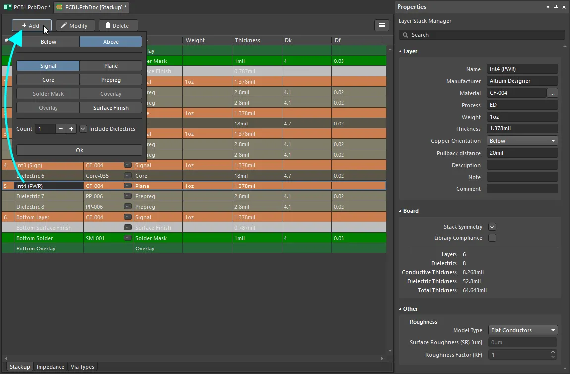
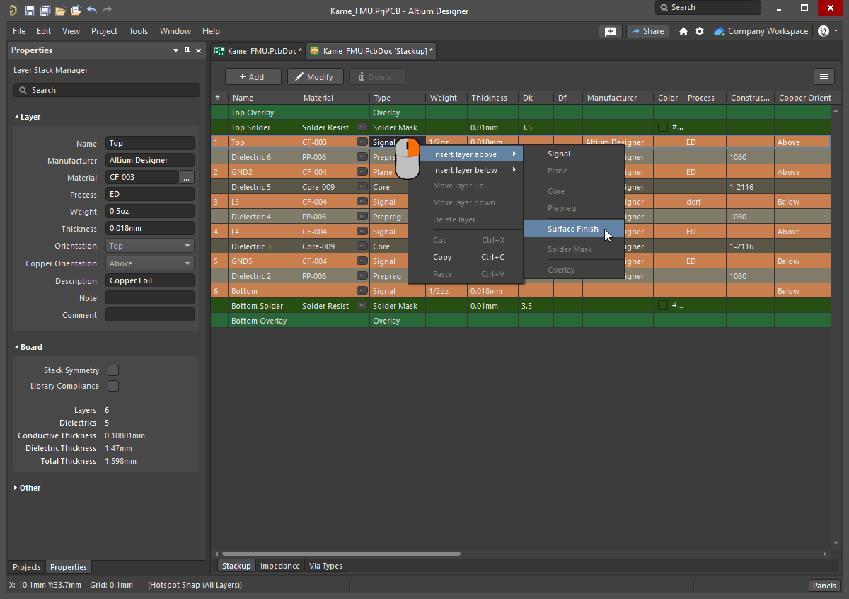
Step 2: Configuring the 6-Layer PCB Stackup in Altium Designer
The layer stackup is the foundation of your 6-layer PCB design. A well-planned stackup ensures proper signal integrity and power distribution. In Altium Designer, access the Layer Stack Manager by going to "Design > Layer Stack Manager." Here, you'll define the six layers and their properties.
For a typical 6-layer PCB, a common stackup configuration is:
- Layer 1: Top Signal Layer
- Layer 2: Ground Plane
- Layer 3: Inner Signal Layer 1
- Layer 4: Inner Signal Layer 2
- Layer 5: Power Plane
- Layer 6: Bottom Signal Layer
This arrangement places ground and power planes between signal layers to minimize crosstalk and provide a stable reference for high-speed signals. In the Layer Stack Manager, set the dielectric material (often FR-4) and thickness for each layer. For instance, signal layers might be 0.1 mm thick, while dielectric layers between them could be 0.3 mm to achieve the total 1.6 mm board thickness.
Enable the "Stack Symmetry" option in the Properties panel to ensure the stackup is balanced, which helps avoid warping during manufacturing. Once configured, save your stackup settings.
Step 3: Placing Components for Optimal Layout
With your stackup defined, import your schematic into the PCB editor by selecting "Design > Import Changes from Schematic." This transfers your components to the PCB layout area. Arrange the components logically to minimize trace lengths and avoid signal interference. Group related components, like power supply circuits or high-speed signal sections, together.
For a 6-layer PCB, place critical components on the top and bottom layers (Layers 1 and 6) to access them easily for routing. Keep sensitive analog components away from noisy digital circuits to reduce interference. Use Altium’s 3D view to check for mechanical fit and ensure components align with your enclosure design.
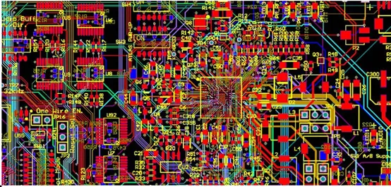
Step 4: Routing Traces in a 6-Layer PCB with Altium Designer
Routing is a critical step in Altium Designer 6-layer PCB routing. Start by assigning nets to specific layers based on their function. High-speed signals should be routed on inner layers (Layers 3 and 4) adjacent to ground or power planes to control impedance and reduce noise. Low-speed or less critical signals can use the top and bottom layers.
Use Altium’s Interactive Routing tool by selecting "Route > Interactive Routing." Set routing rules in the "PCB Rules and Constraints Editor" to enforce minimum trace widths (e.g., 0.2 mm for signal traces) and clearances (e.g., 0.15 mm) based on your design needs and manufacturing capabilities. For differential pairs, often used in high-speed designs like USB or Ethernet, maintain equal trace lengths and consistent spacing (e.g., 0.1 mm) to ensure signal timing.
Route power traces on the dedicated power plane (Layer 5) to provide a low-impedance path. Avoid splitting planes unnecessarily, as this can disrupt current return paths and cause EMI issues. Use vias to connect components to inner layers, but minimize via count to reduce signal degradation.
Step 5: Ensuring Signal Integrity in Your 6-Layer PCB Design
Signal integrity is a top priority in Altium Designer 6-layer PCB signal integrity. Poor signal integrity can lead to data errors, timing issues, or system failures, especially in high-speed designs. Altium Designer offers tools to simulate and analyze signal behavior before manufacturing.
First, control impedance by matching trace widths and layer spacing to your target impedance value, such as 50 ohms for single-ended signals or 100 ohms for differential pairs. Use the Layer Stack Manager to calculate impedance based on dielectric constants (typically 4.2 for FR-4) and trace geometry. Adjust trace widths if needed to meet these values.
Next, minimize crosstalk by keeping high-speed traces away from each other or routing them on different layers. Add ground vias near signal vias to provide a return path and reduce loop inductance. Use Altium’s Signal Integrity Analyzer to simulate reflections and crosstalk, ensuring signals maintain clean edges without overshoot or ringing.
Step 6: Optimizing Power Distribution in a 6-Layer PCB
Effective power distribution is essential for a stable design, and Altium Designer 6-layer PCB power distribution tools make this process seamless. In a 6-layer PCB, dedicate Layer 5 to power distribution, splitting it into multiple voltage domains if needed (e.g., 3.3V and 5V sections). Use wide traces or plane areas to minimize resistance and ensure even current delivery.
Place decoupling capacitors close to power pins of ICs to filter noise. For instance, use 0.1 μF capacitors for high-frequency noise suppression, connecting them with short traces to the power and ground planes. Via stitching—adding multiple vias around power planes—helps maintain low impedance and reduces voltage drops across the board.
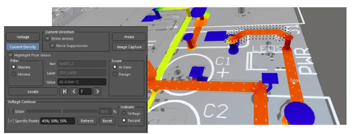
Altium Designer’s Power Distribution Network (PDN) Analyzer can simulate voltage drops and current density. Aim for voltage drops below 1% of the supply voltage (e.g., less than 0.033V for a 3.3V rail) to ensure stability. Adjust plane shapes or add more vias if the analysis shows hot spots or insufficient current capacity.
Step 7: Design Rule Checks and Validation
Before finalizing your design, run a Design Rule Check (DRC) in Altium Designer to catch errors like clearance violations, unconnected nets, or incorrect layer assignments. Go to "Tools > Design Rule Check" and configure rules based on your manufacturer’s specifications, such as minimum drill sizes (e.g., 0.3 mm) and annular ring dimensions (e.g., 0.2 mm).
Review the DRC report and fix any issues. Additionally, use the 3D view to inspect for component height conflicts or mechanical interferences. This step ensures your 6-layer PCB design is ready for manufacturing without costly rework.
Step 8: Generating Outputs for Manufacturing
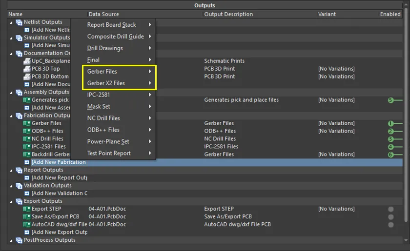
Once your design passes all checks, generate the necessary output files for manufacturing. In Altium Designer, go to "File > Fabrication Outputs > Gerber Files" to export layer-by-layer data. Include a drill file (NC Drill) for via and hole locations. Export a Bill of Materials (BOM) and assembly drawings to assist with component procurement and placement.
Double-check your outputs against your manufacturer’s requirements, such as file formats or layer naming conventions. Many manufacturers provide design guidelines to ensure compatibility with their processes, so align your files accordingly.
Tips for a Successful 6-Layer PCB Design
Here are some additional pointers to enhance your design process:
- Plan Ahead: Sketch your layer stackup and routing strategy before starting to avoid major revisions.
- Use Reference Planes: Always route high-speed signals next to a ground plane to maintain consistent impedance.
- Simulate Early: Run signal integrity and power distribution simulations during the design phase, not just at the end.
- Document Everything: Add notes and labels in Altium Designer to clarify net names and layer functions for future reference.
Conclusion
Designing a 6-layer PCB with Altium Designer can seem daunting, but with this Altium Designer 6-layer PCB tutorial, you have a clear roadmap to success. From setting up your Altium Designer 6-layer PCB stackup to mastering Altium Designer 6-layer PCB routing, ensuring Altium Designer 6-layer PCB signal integrity, and optimizing Altium Designer 6-layer PCB power distribution, each step builds toward a reliable, high-performance board.
Altium Designer’s intuitive tools simplify complex tasks, letting you focus on innovation rather than troubleshooting. Follow the steps outlined in this guide, leverage simulations, and adhere to best practices to create a 6-layer PCB that meets your project’s demands. With careful planning and execution, your design will be ready for manufacturing in no time.


