 ALLPCB


If you're an engineer looking to master the rigid-flex PCB assembly process, you're in the right place. Rigid-flex PCBs combine the benefits of rigid and flexible circuits, offering durability and adaptability for complex electronic designs. This guide will walk you through every step of the assembly process, from design to inspection, while addressing key challenges, equipment needs, and defect prevention. Whether you're working on aerospace, medical, or consumer electronics projects, this detailed resource will help you achieve high-quality results with confidence.
In the sections below, we'll dive deep into the rigid-flex PCB assembly process, explore the essential equipment, tackle common challenges, identify potential defects, and outline inspection techniques to ensure flawless outcomes. Let's get started on building your expertise in this innovative technology.
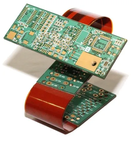
What is Rigid-Flex PCB Assembly?
Rigid-flex PCB assembly involves the integration of rigid and flexible circuit boards into a single unit. These hybrid boards are designed to save space, reduce weight, and improve reliability in applications where traditional rigid boards or separate flex circuits fall short. Think of devices like foldable smartphones or wearable medical sensors—these often rely on rigid-flex technology to function effectively in compact or dynamic environments.
The assembly process is more complex than standard PCB manufacturing due to the combination of materials and the need for precise alignment between rigid and flexible sections. Engineers must account for unique design constraints, material properties, and manufacturing techniques to ensure the final product performs as expected. In this guide, we'll break down each stage of the process to help you navigate these complexities.
Why Choose Rigid-Flex PCBs?
Before diving into the assembly steps, it's worth understanding why rigid-flex PCBs are a game-changer. They offer several advantages:
- Space Efficiency: By folding or bending, they fit into tight spaces, reducing the need for connectors and cables.
- Durability: Fewer interconnects mean fewer points of failure, enhancing reliability.
- Weight Reduction: Ideal for portable or lightweight devices, such as drones or wearables.
- Signal Integrity: With shorter signal paths, they can support high-speed data transfer, often exceeding 5 Gbps in modern designs.
Now, let's explore the rigid-flex PCB assembly process in detail to help you master every aspect of production.
Step-by-Step Guide to Rigid-Flex PCB Assembly Process
The rigid-flex PCB assembly process requires careful planning and execution. Below, we've outlined the key steps to ensure a successful outcome for your project.
Step 1: Design and Layout Planning
The foundation of any rigid-flex PCB starts with a well-thought-out design. Engineers must consider the placement of rigid and flexible sections, ensuring that bend areas are free from components or vias that could crack under stress. Use design software to simulate bending and verify that the flex areas can withstand a minimum bend radius—often as tight as 10 times the thickness of the flex material (e.g., 0.1 mm for a 0.01 mm thick layer).
Key considerations include:
- Layer stack-up: Define the number of layers (often 4-12 for complex designs) and materials, such as polyimide for flex sections and FR-4 for rigid areas.
- Impedance control: Maintain consistent impedance (e.g., 50 ohms for high-speed signals) across transitions between rigid and flex zones.
- Thermal management: Plan for heat dissipation in rigid areas to prevent damage to flex materials, which typically have lower thermal tolerance.
Step 2: Material Selection and Preparation
Choosing the right materials is critical for rigid-flex PCB assembly. Flexible sections often use polyimide films with thicknesses ranging from 0.025 mm to 0.125 mm, while rigid sections rely on standard FR-4 or high-Tg materials for stability. Adhesives or bonding sheets must be selected to ensure strong lamination without compromising flexibility.
During preparation, materials are cut and cleaned to remove contaminants. This step is crucial to prevent delamination, a common defect in rigid-flex boards, especially under thermal stress during soldering.
Step 3: Lamination and Layer Bonding
Lamination binds the rigid and flexible layers into a cohesive unit. This process uses heat (often 180-200°C) and pressure to fuse materials with adhesives or prepreg layers. Precision is key—misalignment by even 0.1 mm can lead to signal issues or mechanical failure in the flex areas.
Special attention is given to the transition zones between rigid and flex sections. These areas are prone to stress, so manufacturers often reinforce them with additional coverlay or stiffeners.
Step 4: Drilling and Plating
Drilling creates vias and through-holes for electrical connections. For rigid-flex PCBs, laser drilling is often used in flex areas to achieve precise microvias (diameters as small as 0.05 mm), while mechanical drilling handles rigid sections. After drilling, holes are plated with copper (typically 25-35 μm thick) to ensure conductivity across layers.
Challenges arise in maintaining hole wall integrity in flex materials, as they are softer and more prone to tearing. Specialized cleaning processes, like plasma etching, are used to remove debris and ensure reliable plating.
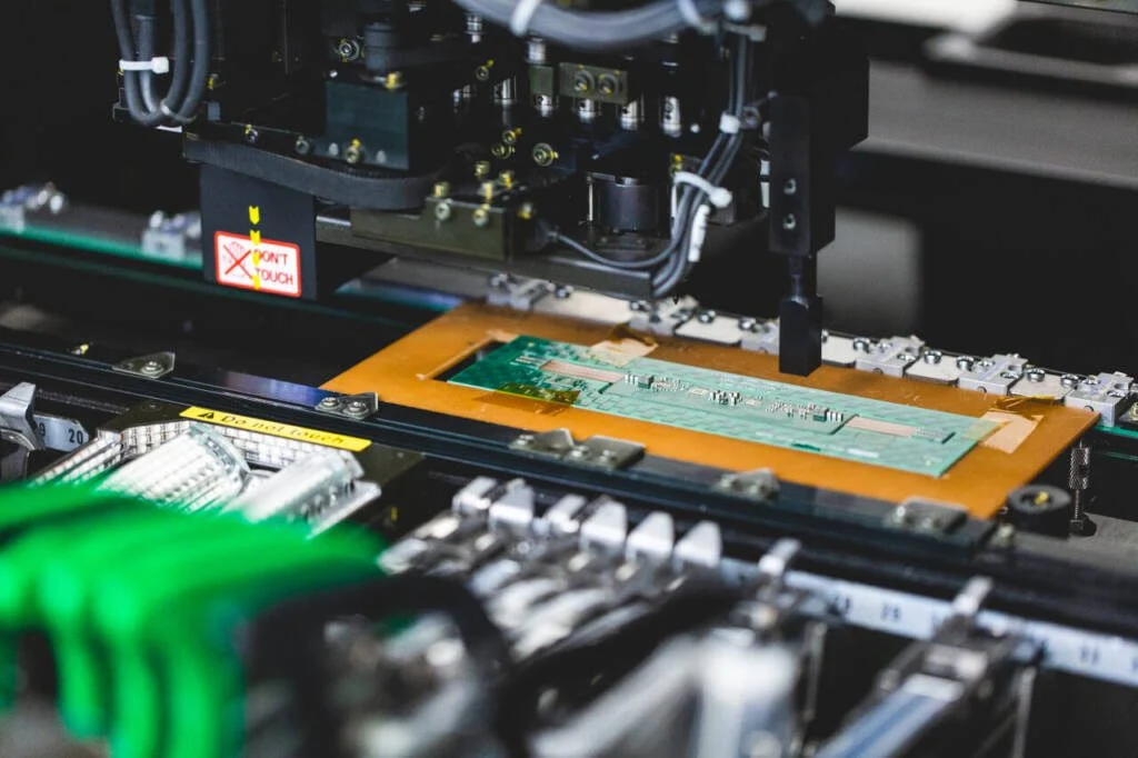
Step 5: Component Placement and Soldering
Component placement in rigid-flex PCB assembly requires automated pick-and-place machines for accuracy. Surface-mount technology (SMT) is commonly used, with components placed only on rigid sections to avoid stress on flexible areas. Reflow soldering follows, using controlled temperature profiles (peak temperatures around 245°C for lead-free solder) to bond components without damaging the flex substrate.
Step 6: Testing and Inspection
Testing ensures the assembled rigid-flex PCB meets design specifications. Electrical tests check for continuity and impedance, while functional tests simulate real-world operation. Inspection techniques, which we'll cover in more detail later, are critical for detecting defects like cracks or misalignment.
Rigid-Flex PCB Assembly Equipment: Tools You Need
The right equipment is essential for successful rigid-flex PCB assembly. Below are the key tools and machines used in the process, tailored to handle the unique requirements of hybrid boards.
- Lamination Presses: These apply heat and pressure to bond layers, with precise control over temperature (up to 200°C) and pressure (up to 500 psi) to prevent material distortion.
- Laser Drilling Systems: Used for creating microvias in flex areas, offering precision down to 0.025 mm for high-density designs.
- Pick-and-Place Machines: Automated systems for accurate component placement, capable of handling components as small as 0.4 mm x 0.2 mm.
- Reflow Ovens: Provide controlled heating profiles for soldering, ensuring temperatures stay within safe limits (e.g., below 260°C) to protect flex materials.
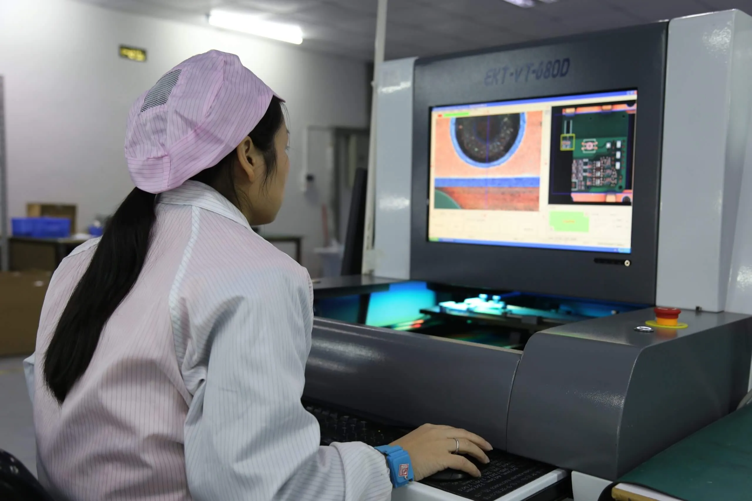
- Automated Optical Inspection (AOI) Systems: Detect surface defects like misaligned components or solder issues with high-resolution cameras.
Investing in high-quality equipment reduces the risk of errors and improves production efficiency, especially for complex rigid-flex designs.
Rigid-Flex PCB Assembly Challenges and How to Overcome Them
Rigid-flex PCB assembly comes with unique challenges due to the combination of materials and design complexity. Here are the most common issues and strategies to address them.
Challenge 1: Material Mismatch and Delamination
The differing thermal expansion rates of rigid (FR-4, ~14 ppm/°C) and flexible (polyimide, ~20 ppm/°C) materials can cause delamination during soldering or operation. To prevent this, use compatible adhesives and ensure uniform heating during lamination.
Challenge 2: Flex Area Stress and Cracking
Repeated bending can lead to cracks in the flex areas, especially near transitions. Design with generous bend radii (at least 10x the material thickness) and add stiffeners to reinforce high-stress zones.
Challenge 3: Alignment Issues
Misalignment between rigid and flex layers can disrupt electrical connections. Use precision fixtures during lamination and drilling to maintain tolerances within 0.05 mm.
Challenge 4: Thermal Management
Flex materials have lower heat tolerance than rigid substrates, risking damage during reflow. Optimize soldering profiles to minimize peak temperatures and use thermal relief designs in high-heat areas.
Common Rigid-Flex PCB Assembly Defects to Watch For
Defects in rigid-flex PCB assembly can compromise performance and reliability. Here are the most frequent issues and their causes.
- Delamination: Occurs due to poor bonding or thermal stress, often visible as separation between layers.
- Cracks in Flex Areas: Result from excessive bending or poor design, leading to broken traces or vias.
- Solder Joint Failures: Caused by uneven heating or contamination, resulting in weak connections.
- Misaligned Layers: Leads to connectivity issues, often due to improper fixturing during manufacturing.
- Copper Plating Defects: Incomplete plating in vias can cause open circuits, often from inadequate cleaning post-drilling.
Early detection of these defects through rigorous inspection is vital to maintaining quality.
Rigid-Flex PCB Assembly Inspection Techniques
Inspection ensures that rigid-flex PCBs meet quality standards before deployment. Below are the primary methods used to identify defects and ensure reliability.
Visual Inspection
The first line of defense, visual inspection checks for obvious defects like delamination or component misalignment. Magnification tools (up to 10x) help spot subtle issues in flex areas.
Automated Optical Inspection (AOI)
AOI systems use high-resolution cameras to detect surface-level defects, such as solder bridges or missing components, with accuracy down to 0.01 mm. This method is fast and ideal for high-volume production.
X-Ray Inspection
For internal defects, X-ray systems reveal issues like voiding in solder joints or misaligned vias. This is especially useful for multilayer rigid-flex boards where visual inspection falls short.
In-Circuit Testing (ICT)
ICT verifies electrical performance by checking for shorts, opens, and correct component values. It ensures signal integrity across the board, often testing impedance within ±10% of the target (e.g., 50 ohms).
Functional Testing
This final step simulates real-world conditions to confirm the board operates as intended. For high-speed designs, engineers might test signal speeds up to 10 Gbps to validate performance.
Best Practices for Successful Rigid-Flex PCB Assembly
To wrap up, here are some proven tips to ensure success in your rigid-flex PCB projects:
- Collaborate closely with your manufacturing team during the design phase to align on material and process capabilities.
- Prioritize prototyping to test bend radii and thermal performance before full-scale production.
- Invest in advanced inspection tools like AOI and X-ray systems to catch defects early.
- Document every step of the assembly process to identify and address recurring issues over time.
- Stay updated on industry standards, such as IPC-2223 for flex and rigid-flex design, to ensure compliance.
Conclusion
Mastering rigid-flex PCB assembly is a valuable skill for engineers working on cutting-edge electronics. By following this step-by-step guide, you can navigate the complexities of the rigid-flex PCB assembly process, from design and material selection to inspection and defect prevention. Understanding the required equipment, anticipating challenges, and implementing robust inspection techniques will help you deliver high-quality, reliable boards for any application.
With the right approach, rigid-flex technology opens up endless possibilities for compact, durable, and high-performance designs. Keep refining your process, stay attuned to advancements in materials and equipment, and leverage the insights shared here to elevate your engineering projects to the next level.


