 ALLPCB


Scaling from a single-sided PCB prototype to mass production can be a daunting task, but with the right approach, it’s entirely achievable. Whether you're an engineer or a business looking to optimize your single-sided PCB mass production, this guide will walk you through the key steps of scaling PCB assembly, streamlining the PCB manufacturing process, and achieving production optimization. In this comprehensive blog, we’ll cover everything from design considerations to assembly techniques, ensuring your transition to large-scale manufacturing is smooth and efficient.
Understanding Single-Sided PCBs: The Foundation of Scaling
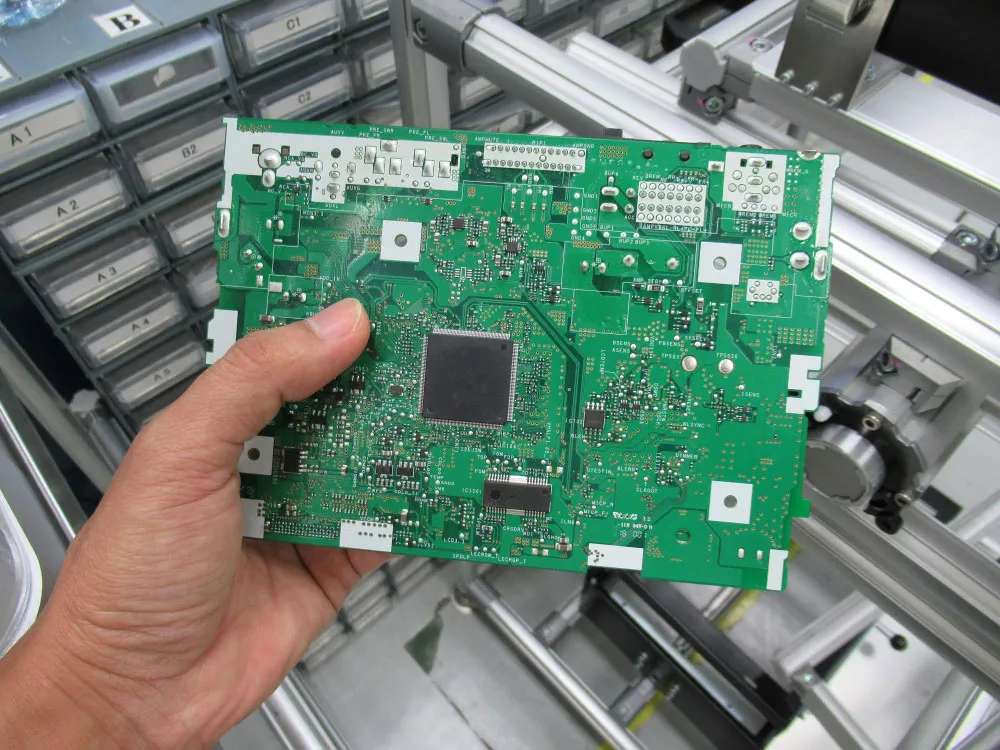
Single-sided PCBs are the simplest type of printed circuit boards, featuring conductive traces on only one side of the board. They are widely used in basic electronics, such as calculators, LED lighting, and power supplies, due to their cost-effectiveness and ease of production. However, when scaling from a prototype to mass production, even these straightforward boards require careful planning to maintain quality and efficiency.
The key to successful single-sided PCB mass production lies in understanding the limitations and strengths of this design. For instance, single-sided boards are less complex than double-sided or multilayer boards, which means fewer manufacturing steps and lower costs. However, they can face challenges with component density and signal integrity if not designed properly for larger volumes.
Step 1: Optimizing Design for Manufacturability (DFM)
Before diving into mass production, the first step in scaling PCB assembly is ensuring your design is ready for manufacturing. Design for Manufacturability (DFM) is a critical concept that focuses on creating a PCB layout that minimizes errors and reduces costs during production.
- Component Placement: Place components on one side of the board to avoid complications during assembly. Ensure there’s enough spacing between components to prevent soldering issues. A minimum spacing of 0.1 inches (2.54 mm) between components is often recommended for automated assembly.
- Trace Width and Spacing: Use appropriate trace widths to handle the required current. For example, a trace width of 0.01 inches (0.254 mm) can carry up to 0.5 amps for a 1 oz copper layer. Maintain a minimum spacing of 0.006 inches (0.152 mm) between traces to avoid short circuits during high-volume runs.
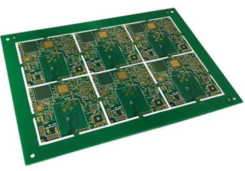
- Panelization: Design your PCB to fit into a panel layout for mass production. This means arranging multiple boards on a single panel to maximize efficiency during fabrication and assembly. Include breakaway tabs or V-scoring for easy separation after production.
By adhering to DFM guidelines, you can prevent costly redesigns and ensure a smoother transition to large-scale manufacturing. This step is foundational for production optimization and sets the stage for efficient assembly processes.
Step 2: Material Selection for Cost and Performance
Material choice plays a significant role in the PCB manufacturing process, especially when scaling to mass production. For single-sided PCBs, the most common substrate material is FR-4, a fiberglass-epoxy laminate that offers a good balance of cost and durability. However, depending on your application, you might consider other materials like CEM-1 or phenolic boards for even lower costs, though they may compromise on performance.
Copper thickness is another critical factor. Standard copper weights for single-sided PCBs are 1 oz (35 μm) or 2 oz (70 μm) per square foot. Thicker copper can handle higher currents but increases costs. For example, a 1 oz copper layer is sufficient for most low-power applications, while 2 oz may be necessary for power supplies with currents exceeding 2 amps.
Selecting the right materials not only impacts the performance of your PCB but also affects production costs at scale. Working closely with your manufacturing partner to choose cost-effective yet reliable materials is a key aspect of production optimization.
Step 3: Streamlining the PCB Manufacturing Process
The PCB manufacturing process for single-sided boards involves several steps, each of which must be optimized for mass production. Here’s a breakdown of the core stages and how to scale them effectively:
- Substrate Preparation: The raw material is cut into the required size and cleaned to remove contaminants. For mass production, automated cutting and cleaning systems can significantly reduce time and labor costs.
- Copper Etching: A photoresist layer is applied, and UV light is used to transfer the circuit pattern onto the board. Unwanted copper is then etched away. High-volume production often uses advanced etching machines to ensure precision and consistency across thousands of boards.
- Drilling: Holes for through-hole components and vias (if any) are drilled. Automated drilling systems can handle hundreds of boards per hour, ensuring uniformity in large batches.
- Surface Finish: A protective finish like HASL (Hot Air Solder Leveling) or ENIG (Electroless Nickel Immersion Gold) is applied to prevent oxidation. HASL is often preferred for single-sided PCBs due to its lower cost, though ENIG offers better reliability for fine-pitch components.
- Silkscreen and Testing: Component labels are printed on the board, and electrical testing (like flying probe or bed-of-nails testing) ensures functionality. Automated testing systems are essential for mass production to maintain quality control.
By investing in automation and standardized processes, manufacturers can achieve higher throughput and lower defect rates, which are crucial for single-sided PCB mass production.
Step 4: Scaling PCB Assembly for High-Volume Production
Once the bare boards are manufactured, the next challenge in scaling PCB assembly is assembling components onto the boards. For single-sided PCBs, assembly is relatively straightforward since components are placed on only one side. However, efficiency and accuracy are critical when producing thousands or millions of units.
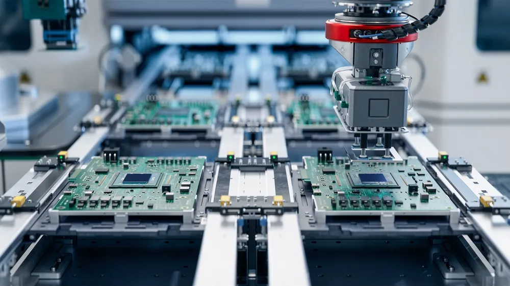
- Surface Mount Technology (SMT): SMT is the preferred method for high-volume assembly. Automated pick-and-place machines can place components at speeds of up to 100,000 components per hour, ensuring rapid production. For single-sided PCBs, SMT simplifies the process since there’s no need for double-sided reflow soldering.
- Through-Hole Technology (THT): For components that require stronger mechanical bonds, like connectors or large capacitors, THT may be used. Wave soldering machines can automate this process for mass production, passing the board over a wave of molten solder to secure through-hole components.
- Inspection and Quality Control: Automated Optical Inspection (AOI) systems can scan assembled boards for defects like misaligned components or soldering issues. For high-volume runs, AOI can inspect thousands of boards per day, ensuring consistent quality.
Scaling assembly also means optimizing the supply chain for components. Bulk purchasing and just-in-time inventory systems can reduce costs and prevent production delays. A well-coordinated assembly line is the backbone of production optimization for mass manufacturing.
Step 5: Testing and Quality Assurance at Scale
Quality assurance is non-negotiable when scaling to mass production. Even a small defect rate can lead to significant losses in high-volume runs. For single-sided PCB mass production, testing must be both thorough and efficient.
In-Circuit Testing (ICT) is commonly used to verify the functionality of assembled boards. ICT checks for shorts, opens, and component values, ensuring each board meets specifications. For a batch of 10,000 boards, ICT can reduce defective units to less than 0.1% if implemented correctly.
Functional testing is another critical step, especially for applications where reliability is paramount. This involves powering up the board and simulating real-world conditions to ensure it performs as expected. Automated test fixtures can handle large volumes, testing hundreds of boards per hour.
By integrating robust testing protocols into the PCB manufacturing process, you can maintain high quality while meeting the demands of mass production.
Step 6: Logistics and Cost Management for Mass Production
Scaling to mass production isn’t just about manufacturing—it’s also about managing logistics and costs. Efficient production optimization requires careful planning in the following areas:
- Inventory Management: Maintain an optimal stock of raw materials and components to avoid production halts. Overstocking ties up capital, while understocking risks delays.
- Shipping and Distribution: Plan bulk shipping to reduce transportation costs. For international markets, consider regional assembly to minimize shipping times and tariffs.
- Cost Reduction Strategies: Negotiate bulk pricing with suppliers and optimize panel layouts to reduce material waste. Even a 5% reduction in material costs can lead to significant savings over a run of 100,000 boards.
Effective logistics management ensures that your scaled production remains profitable and meets customer deadlines without compromising quality.
Common Challenges in Scaling Single-Sided PCB Production
Even with careful planning, scaling production can present challenges. Here are some common issues and how to address them:
- Design Errors: A small mistake in the prototype phase can become a costly problem in mass production. Always conduct thorough design reviews and prototype testing before scaling.
- Supply Chain Delays: Component shortages can halt production. Build relationships with multiple suppliers to mitigate risks.
- Quality Variability: Inconsistent manufacturing or assembly processes can lead to defects. Standardize processes and invest in automation to maintain consistency.
By anticipating these challenges, you can develop contingency plans to keep your single-sided PCB mass production on track.
Conclusion: Your Path to Successful Mass Manufacturing
Transitioning from prototype to production for single-sided PCBs is a journey that requires attention to detail, strategic planning, and a focus on efficiency. By optimizing your design for manufacturability, selecting the right materials, streamlining the PCB manufacturing process, and scaling PCB assembly, you can achieve production optimization and deliver high-quality boards at scale.
At every stage, partnering with a reliable manufacturing service can make a significant difference. From providing DFM feedback to offering automated assembly and testing, the right partner can help you navigate the complexities of single-sided PCB mass production. Start with a solid foundation, scale smartly, and watch your project grow from a single prototype to a market-ready product.


