 ALLPCB


Component misplacement in PCB assembly is a common yet critical defect that can lead to malfunctioning circuits, costly rework, and delayed production timelines. In this ultimate guide, we’ll explore the causes of component misplacement, its effects on PCB performance, and practical solutions to prevent it. Whether you're an engineer, designer, or manufacturer, this blog will provide actionable insights to tackle PCB assembly defects and ensure high-quality outcomes. Let’s dive into the details of component misplacement and how to address it effectively.
What is Component Misplacement in PCB Assembly?
Component misplacement occurs when electronic components are incorrectly positioned on a printed circuit board (PCB) during the assembly process. This defect can happen due to human error, machine misalignment, or design flaws, leading to issues like poor electrical connections or complete circuit failure. As PCBs become more complex with smaller components and tighter tolerances, the risk of misplacement increases, making it a significant concern in modern electronics manufacturing.
Common Causes of Component Misplacement in PCB Assembly
Understanding the root causes of component misplacement is the first step in preventing this defect. Below are the most frequent reasons for misplacement during PCB assembly:
1. Human Error in Manual Assembly
In manual or semi-automated assembly processes, human error is a leading cause of component misplacement. Workers may misinterpret design files or place components in the wrong orientation, especially when handling small parts like 0402 or 0201 surface-mount devices (SMDs). Fatigue or lack of training can exacerbate these mistakes.
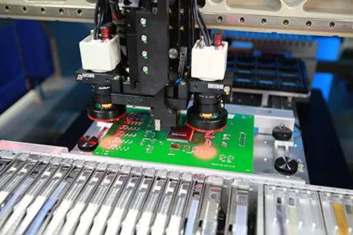
2. Machine Misalignment in Automated Assembly
Automated pick-and-place machines are widely used in high-volume production, but they are not immune to errors. Miscalibration of the machine, incorrect programming, or worn-out nozzles can result in components being placed off-center or rotated incorrectly. For instance, a misalignment of just 0.1 mm can cause connection issues in high-density designs.
3. Incorrect Design Files or Bill of Materials (BOM)
Errors in the design files or BOM can lead to component misplacement. If the footprint in the design software does not match the physical component, or if the BOM lists the wrong part number, the assembly process will be flawed from the start. This is especially common when designs are rushed or not thoroughly reviewed.
4. Component Packaging Issues
Components supplied in incorrect or damaged packaging, such as tape-and-reel or trays, can confuse automated machines or manual assemblers. For example, if a reel is mislabeled with a 1kΩ resistor instead of a 10kΩ one, the wrong part may be placed on the board.
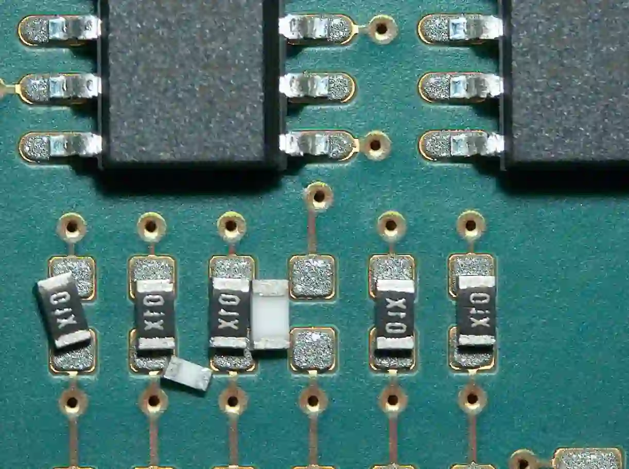
5. Poor PCB Design Practices
Inadequate spacing between components or unclear markings on the PCB layout can contribute to misplacement. If pads are too close together (e.g., less than 0.2 mm apart for SMDs), there’s a higher chance of components overlapping or being placed incorrectly during assembly.
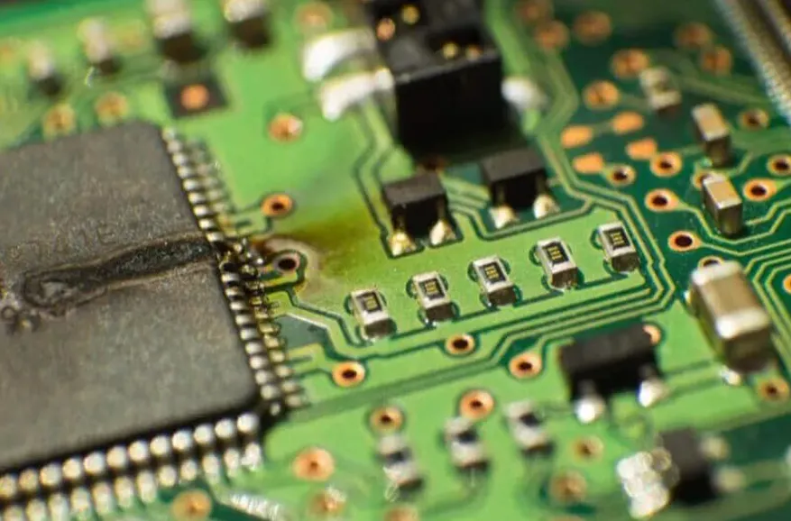
Effects of Component Misplacement on PCB Performance
Component misplacement doesn’t just delay production; it can have severe consequences for the functionality and reliability of the final product. Here’s how this defect impacts PCB performance:
1. Electrical Connection Failures
When a component is misplaced, it may fail to make proper contact with the solder pads, leading to open circuits or intermittent connections. For example, a misplaced capacitor in a power supply circuit could cause voltage instability, with fluctuations exceeding safe limits like ±5%.
2. Short Circuits and Overheating
If a component is placed too close to another or overlaps conductive traces, it can create a short circuit. This often results in overheating, which can damage nearby components or even cause the PCB to fail entirely. In high-power applications, this could lead to thermal runaway, where temperatures exceed 150°C.
3. Signal Integrity Issues
In high-speed digital circuits, component misplacement can disrupt signal integrity. For instance, a misplaced decoupling capacitor near a microcontroller might fail to suppress noise, leading to signal delays or jitter beyond acceptable thresholds (e.g., >50 ps in a 5 GHz signal).
4. Increased Rework Costs and Delays
Detecting and correcting misplaced components often requires manual rework, which is time-consuming and expensive. Rework can cost up to 10 times more than initial assembly, and delays can push back product launches by weeks or months.
5. Reduced Product Reliability
Even if a misplaced component is fixed, the rework process can introduce new defects like solder joint cracks or thermal stress. This reduces the overall reliability of the product, potentially leading to field failures and customer dissatisfaction.
Solutions to Prevent Component Misplacement in PCB Assembly
Preventing component misplacement requires a combination of good design practices, robust manufacturing processes, and thorough quality checks. Below are practical solutions to minimize PCB assembly defects caused by misplacement:
1. Optimize PCB Design for Assembly (DFA)
Design for Assembly (DFA) principles can significantly reduce the risk of misplacement. Ensure that component footprints match the physical parts exactly, and provide adequate spacing (e.g., at least 0.3 mm between SMD pads) to avoid overlap. Clear silkscreen markings for polarity and orientation also help assemblers place components correctly.
2. Use Automated Optical Inspection (AOI)
Automated Optical Inspection systems can detect misplaced components after placement but before soldering. AOI machines use high-resolution cameras to verify component positions with an accuracy of up to 0.01 mm, catching errors early in the process and reducing rework costs by as much as 30%.
3. Implement Strict Quality Control for Design Files
Before assembly begins, double-check design files and the BOM for accuracy. Use design rule checks (DRC) in your PCB design software to identify potential issues like mismatched footprints or incorrect part numbers. A thorough review can prevent up to 80% of design-related misplacement errors.
4. Calibrate and Maintain Pick-and-Place Machines
Regular calibration of pick-and-place machines ensures precise component placement. Schedule maintenance checks to inspect nozzles, vision systems, and alignment mechanisms. For high-density boards, aim for a placement accuracy of ±0.05 mm to meet industry standards.
5. Train Assembly Personnel
For manual or semi-automated assembly, invest in training programs for workers. Teach them to read design files accurately, recognize component polarities, and handle small parts with precision. Well-trained staff can reduce human error by up to 50% in manual assembly processes.
6. Verify Component Packaging
Before assembly, inspect component packaging to ensure it matches the BOM. Use barcode scanning or visual checks to confirm that reels, trays, or tubes contain the correct parts. This simple step can eliminate misplacement caused by packaging errors.
7. Conduct Post-Assembly Testing
After assembly, perform functional testing and in-circuit testing (ICT) to identify any issues caused by misplaced components. ICT can detect open circuits or shorts with a detection rate of over 95%, ensuring that defective boards don’t reach the market.
How to Address Component Misplacement When It Occurs
Despite best efforts, component misplacement can still happen. When it does, follow these steps to address the issue efficiently:
1. Identify the Misplacement
Use AOI or visual inspection to locate the misplaced component. Compare the physical board with the design files to confirm the error. For complex boards, X-ray inspection can help identify issues hidden under larger components.
2. Remove and Reposition the Component
Use a rework station with a hot air gun or soldering iron to carefully remove the misplaced component. Clean the pads with isopropyl alcohol and a brush to remove old solder, then reposition the component accurately using tweezers or a vacuum tool.
3. Resolder and Inspect
Apply fresh solder paste or flux and resolder the component in the correct position. After soldering, inspect the board again with AOI or a magnifying glass to ensure proper alignment and solder joint quality.
4. Test the Board
Run functional tests to verify that the correction resolved the issue without introducing new defects. Check for signal integrity, voltage levels, and thermal performance to confirm the board meets specifications.
Why Preventing Component Misplacement Matters
Preventing component misplacement is not just about avoiding immediate defects; it’s about ensuring long-term reliability and customer trust. A single misplaced component can lead to product recalls, costing companies thousands or even millions of dollars. By investing in prevention strategies, manufacturers can achieve higher first-pass yields (often above 98%) and reduce waste, ultimately saving time and resources.
Conclusion: Mastering PCB Assembly with Precision
Component misplacement is a significant challenge in PCB assembly, but with the right strategies, it can be effectively managed. By addressing the causes—such as human error, machine misalignment, and design flaws—you can minimize the effects like electrical failures and costly rework. Implementing solutions like DFA, AOI, and thorough training ensures that your PCBs meet the highest quality standards.


