ALLPCB


In the world of printed circuit board (PCB) fabrication, every design decision impacts the final cost. One critical factor that often goes under the radar is tight trace-to-pad spacing. So, what is the cost impact of tight trace-to-pad spacing in PCB fabrication? Simply put, tighter spacing between traces and pads can increase manufacturing costs due to higher precision requirements, advanced equipment needs, and a greater risk of defects during production. However, it can also enable layer reduction and space optimization, potentially lowering costs in specific scenarios.
In this comprehensive guide, we’ll dive deep into how tight trace-to-pad spacing influences PCB cost optimization, explore its role in manufacturing processes, and provide actionable insights for leveraging Design for Manufacturability (DFM) principles. Whether you’re an engineer working on a high-density design or a project manager aiming to balance quality and budget, understanding these factors is key to making informed decisions.
Understanding Trace-to-Pad Spacing in PCB Design
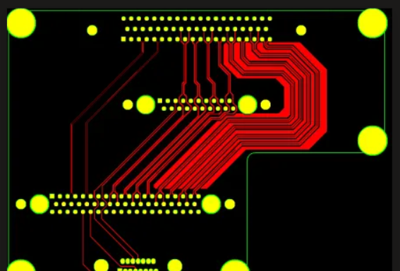
Trace-to-pad spacing refers to the distance between a conductive trace (the copper pathways that carry electrical signals) and a pad (the area where components are soldered onto the PCB). This spacing is critical for preventing electrical interference, ensuring signal integrity, and maintaining manufacturability. In modern electronics, where devices are becoming smaller and more complex, designers often push for tighter spacing to fit more components into limited board real estate.
While tighter spacing can help achieve compact designs, it comes with trade-offs. Manufacturing a PCB with minimal trace-to-pad spacing requires precision tools and processes, which can drive up costs. Let’s break down the specific ways this design choice impacts fabrication expenses and explore strategies for balancing performance with budget.
How Tight Trace-to-Pad Spacing Affects PCB Fabrication Costs
When designing a PCB, the spacing between traces and pads directly influences the complexity of the manufacturing process. Here are the primary ways tight spacing impacts costs:
1. Increased Manufacturing Precision Requirements
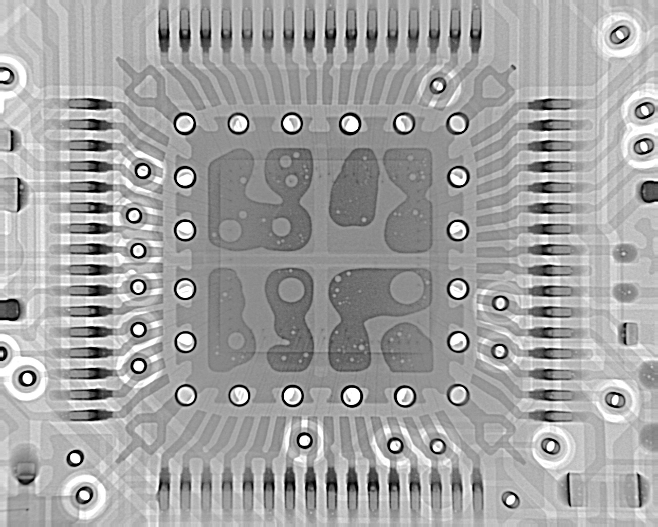
Tight trace-to-pad spacing demands high-precision equipment to etch copper layers and place components without errors. For instance, standard spacing might be around 6 mils (0.006 inches), but high-density designs often reduce this to 3 mils or less. Achieving such precision requires advanced machinery, like laser direct imaging (LDI) systems, which are more expensive to operate than traditional photolithography tools. This translates to higher fabrication costs per board.
Additionally, tighter tolerances mean that manufacturers must implement stricter quality control measures. Each board may need extra inspection steps, such as automated optical inspection (AOI), to detect potential defects like shorts or open circuits caused by insufficient spacing.
2. Higher Risk of Defects and Yield Loss
Smaller spacing increases the risk of manufacturing defects. If a trace is too close to a pad, even a slight misalignment during etching or soldering can cause a short circuit. According to industry data, defect rates can rise by 10-15% when spacing drops below 4 mils without corresponding adjustments in process control. Higher defect rates lead to lower yields, meaning more boards are scrapped or require rework, ultimately increasing production costs.
3. Impact on Material and Process Selection
Tight spacing often necessitates the use of specialized materials, such as high-frequency laminates or thinner copper foils, to maintain signal integrity and prevent crosstalk. These materials are typically more expensive than standard FR-4 substrates. Furthermore, manufacturers may need to use finer line widths and spaces, which can require additional process steps like micro-etching, adding to the overall expense.
Balancing Tight Spacing with PCB Cost Optimization
While tight trace-to-pad spacing can increase costs, it also offers opportunities for PCB cost optimization when approached strategically. Here’s how designers can minimize expenses while achieving the desired performance:
1. Leverage Design for Manufacturability (DFM) Principles
Design for Manufacturability (DFM) focuses on creating PCB layouts that are easy and cost-effective to produce. When dealing with tight spacing, DFM guidelines suggest maintaining a balance between density and manufacturability. For example, consult with your fabrication partner early in the design phase to understand their minimum spacing capabilities. Many manufacturers can handle 4-5 mil spacing at a standard cost, but going below this threshold may trigger premium pricing.
DFM also encourages designers to avoid over-constraining the layout. If tight spacing is only necessary in specific high-density areas, consider relaxing constraints elsewhere on the board to simplify production.
2. Consider Layer Reduction as a Cost-Saving Measure
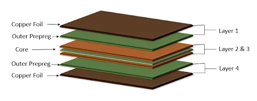
One potential benefit of tight trace-to-pad spacing is the ability to reduce the number of layers in a PCB. By packing more traces into a smaller area, you might fit all necessary connections on fewer layers, cutting material and fabrication costs. For instance, reducing a design from 6 layers to 4 can save up to 20-30% on production expenses, depending on the complexity of the board.
However, this approach requires careful planning. Reducing layers often means tighter spacing across the board, which can negate savings if manufacturing defects increase. Use simulation tools to test signal integrity and ensure that layer reduction doesn’t compromise performance.
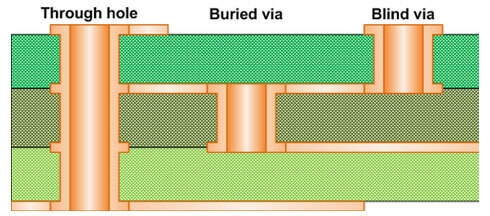
3. Explore Blind and Buried Vias for Space Efficiency
In high-density designs, blind and buried vias can complement tight trace-to-pad spacing by freeing up surface area. Blind vias connect an outer layer to an inner layer without passing through the entire board, while buried vias connect internal layers only. These vias allow for more routing options without increasing board size or layer count, potentially offsetting the costs of tight spacing.
Keep in mind that blind and buried vias are more expensive to fabricate than through-hole vias due to the additional drilling and plating steps involved. A single blind via can cost 2-3 times more than a standard via. Therefore, use them selectively in areas where space constraints are critical.
Manufacturing Processes and Their Role in Managing Tight Spacing Costs
The manufacturing process itself plays a significant role in determining the cost impact of tight trace-to-pad spacing. Understanding these processes can help designers make informed choices that align with budget goals.
1. Etching and Imaging Precision
The etching process, which defines the copper traces on a PCB, becomes more challenging with tighter spacing. Manufacturers often rely on advanced imaging techniques to achieve fine line widths and spaces. For example, achieving 3-mil spacing may require an LDI system with a resolution of 10 microns or better, compared to 50 microns for standard spacing. This precision comes at a higher cost but is necessary for high-density interconnect (HDI) designs.
2. Soldering and Assembly Challenges
During assembly, tight spacing increases the risk of solder bridging, where excess solder creates unintended connections between pads and traces. To mitigate this, manufacturers may use finer solder paste stencils or advanced reflow soldering techniques, both of which add to production costs. For surface-mount components with pitches below 0.5 mm, assembly costs can increase by 15-25% due to the need for specialized equipment.
3. Testing and Quality Assurance
Boards with tight spacing often require more rigorous testing to ensure reliability. Electrical testing, such as in-circuit testing (ICT), becomes more complex and time-consuming, adding to the overall expense. Additionally, manufacturers may need to perform impedance testing to verify signal integrity, especially for high-speed designs where tight spacing can affect performance. Impedance mismatches, if not addressed, can lead to signal delays or data loss.
Practical Tips for Managing Costs with Tight Trace-to-Pad Spacing
Navigating the cost implications of tight spacing doesn’t have to be a daunting task. Here are some practical tips to keep expenses in check while meeting design requirements:
- Start with Manufacturer Guidelines: Before finalizing your design, review the spacing and tolerance guidelines provided by your fabrication partner. Aligning your layout with their capabilities can prevent costly redesigns.
- Use Simulation Tools: Employ PCB design software to simulate signal integrity and identify potential issues with tight spacing. Addressing problems in the design phase is far cheaper than fixing defects during production.
- Prioritize Critical Areas: Reserve tight spacing for high-density sections of the board, such as near microcontrollers or connectors, and use standard spacing elsewhere to reduce overall complexity.
- Optimize Component Placement: Place components strategically to minimize the need for tight spacing. Grouping similar components together can simplify routing and reduce congestion.
- Plan for Scalability: If you anticipate future design iterations, build some flexibility into your spacing constraints to avoid expensive redesigns as requirements evolve.
Conclusion: Striking the Right Balance for Cost and Performance
Tight trace-to-pad spacing in PCB fabrication is a double-edged sword. On one hand, it enables compact, high-performance designs that meet the demands of modern electronics. On the other hand, it can significantly increase manufacturing costs due to the need for precision equipment, specialized materials, and enhanced quality control. By understanding these cost drivers and applying Design for Manufacturability (DFM) principles, engineers can achieve PCB cost optimization without sacrificing quality.
Strategies like layer reduction and the selective use of blind and buried vias can help offset expenses, while close collaboration with your fabrication partner ensures that your design aligns with manufacturing capabilities. Ultimately, the key to success lies in balancing tight spacing with practical cost-saving measures, ensuring that your PCB meets both performance and budget goals.
Armed with these insights, you’re better equipped to navigate the complexities of PCB design and fabrication. Whether you’re working on a simple prototype or a complex multilayer board, thoughtful planning around trace-to-pad spacing can make all the difference in achieving a cost-effective, high-quality product.