ALLPCB


A good PCB stack-up for signal integrity refers to the strategic arrangement of layers in a printed circuit board (PCB) to ensure clean, reliable signal transmission while minimizing noise, interference, and signal loss. It involves carefully organizing signal layers, ground planes, power planes, and dielectric materials to control impedance, provide solid return paths, and reduce electromagnetic interference (EMI). A well-designed stack-up is critical for high-speed designs, ensuring signals travel without distortion and maintaining the overall performance of the circuit.
In this comprehensive guide, we’ll dive deep into the elements that define a good PCB stack-up for signal integrity. We’ll explore the importance of layers, impedance control, return paths, and planes, providing practical insights for engineers and designers looking to optimize their PCB designs.
Why PCB Stack-Up Matters for Signal Integrity
Signal integrity is the backbone of any electronic design, especially in high-speed applications like telecommunications, automotive systems, and consumer electronics. Poor signal integrity can lead to data errors, signal delays, crosstalk, and even complete system failure. The PCB stack-up plays a pivotal role in maintaining signal integrity by determining how signals interact with the board’s layers and materials.
A thoughtfully planned stack-up ensures that high-speed signals travel with minimal interference, controlled impedance, and a clear return path. Without this, signals can degrade due to reflections, noise, or improper grounding. For instance, in a high-speed design operating at 5 GHz, even a small mismatch in impedance (say, 50 ohms versus 55 ohms) can cause significant signal reflection, leading to data loss. Let’s break down the key components of a good PCB stack-up and how they contribute to signal integrity.
Key Elements of a Good PCB Stack-Up for Signal Integrity
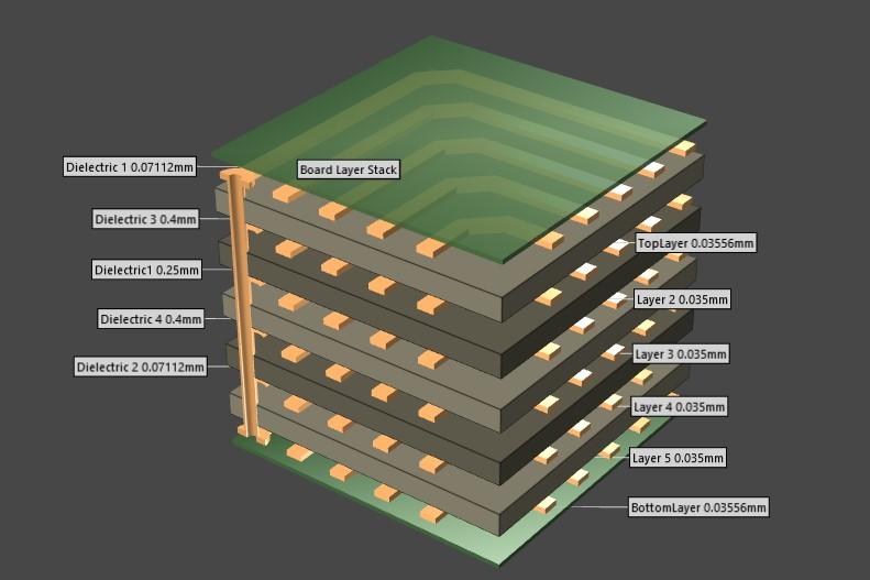
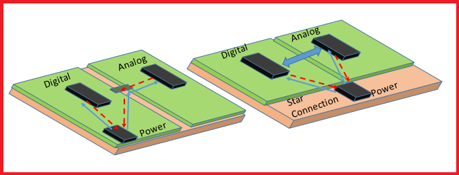
1. Layer Arrangement: Balancing Signals and Planes
The arrangement of layers in a PCB stack-up is the foundation of signal integrity. A typical multi-layer PCB consists of signal layers (for routing traces) and plane layers (for ground and power). The way these layers are ordered directly impacts how signals behave.
For example, in a 4-layer PCB, a common stack-up might look like this:
- Top Layer: Signal (high-speed traces)
- Layer 2: Ground Plane
- Layer 3: Power Plane
- Bottom Layer: Signal (low-speed traces or additional routing)
This arrangement places a ground plane close to the high-speed signal layer, providing a low-impedance return path and reducing noise. In contrast, placing two signal layers next to each other without a separating ground plane can lead to crosstalk, where signals interfere with each other. For a 6-layer or 8-layer PCB, additional signal and plane layers can be added, but the principle remains: keep high-speed signals close to a reference plane (ground or power) to maintain signal integrity.
Tip: Always prioritize symmetry in layer stack-up to avoid board warping during manufacturing. For instance, in an 8-layer board, balance the number of signal and plane layers on both sides of the center.
2. Impedance Control: Matching the Signal Path
Impedance control is a critical factor in a good PCB stack-up for signal integrity. Impedance refers to the resistance a signal encounters as it travels along a trace. If the impedance of a trace doesn’t match the source and load (e.g., a 50-ohm system), signal reflections occur, degrading signal quality.
In a PCB stack-up, impedance is influenced by the trace width, the thickness of the dielectric material between layers, and the proximity to a reference plane. For high-speed designs, such as USB 3.0 or PCIe, maintaining a consistent impedance (often 50 ohms for single-ended signals or 100 ohms for differential pairs) is essential. Designers can use stack-up planning tools to calculate the required trace width and dielectric thickness. For instance, a trace width of 5 mils over a ground plane with a 4-mil dielectric might achieve a 50-ohm impedance in FR-4 material (with a dielectric constant of about 4.2).
To achieve controlled impedance, ensure that signal layers are adjacent to a continuous reference plane. Avoid routing high-speed traces over split planes, as this disrupts impedance and introduces noise.
3. Return Path: Ensuring a Clear Route for Signals
A good PCB stack-up must provide a clear and uninterrupted return path for signals. The return path is the route that the current takes to complete the circuit, typically through a ground plane. If the return path is broken or too far from the signal trace, it can cause signal distortion and EMI.
For high-speed signals, the return path should follow the shortest, most direct route beneath the signal trace on the adjacent ground plane. This minimizes the loop area, reducing inductance and noise. A common mistake in stack-up design is placing a signal layer between two power planes without a nearby ground plane, forcing the return path to take a longer route, which degrades signal integrity.
For example, in a design with a 2.5 GHz signal, a poorly planned return path could increase loop inductance, leading to a voltage spike or signal delay. To avoid this, always ensure high-speed signal layers are next to a solid ground plane in the stack-up.
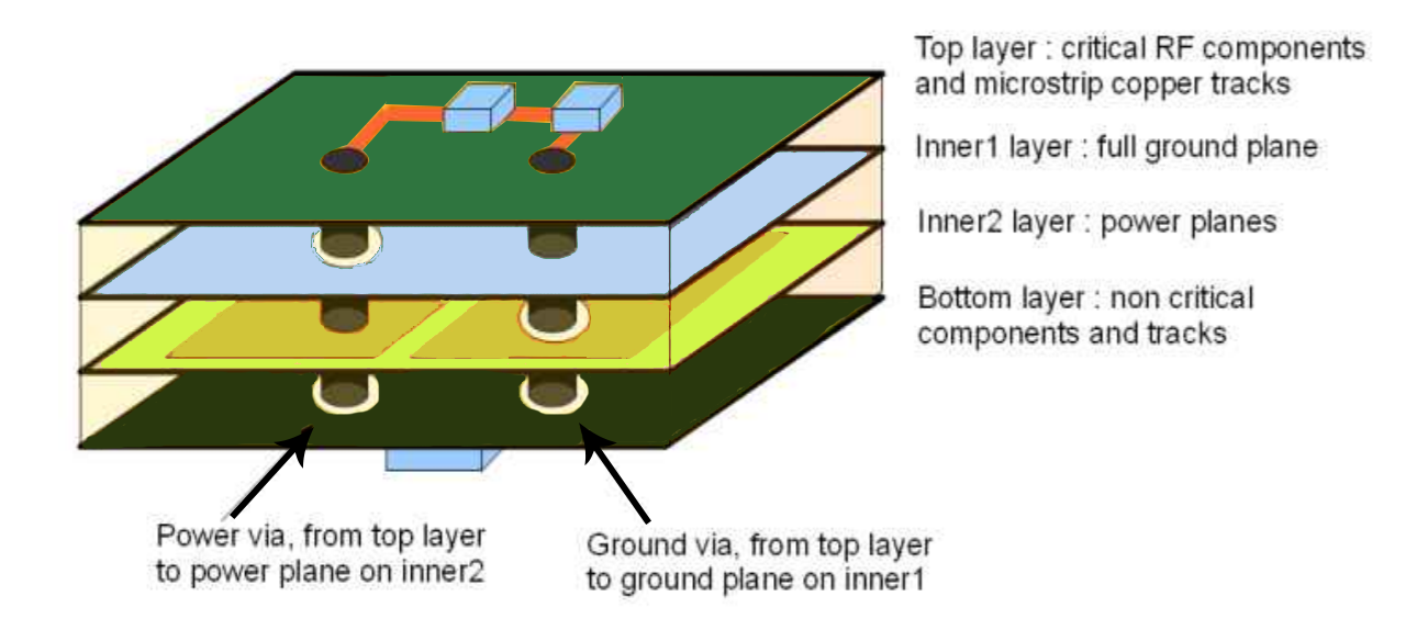
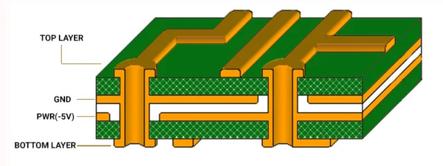
4. Ground and Power Planes: Stabilizing the System
Ground and power planes are essential components of a good PCB stack-up. These continuous copper layers provide stable voltage levels, reduce noise, and serve as reference planes for signal traces. A solid ground plane acts as a shield, absorbing EMI and preventing crosstalk between adjacent signal layers.
In a well-designed stack-up, ground planes should be placed strategically to separate signal layers. For instance, in a 6-layer PCB, you might have:
- Top Layer: Signal
- Layer 2: Ground Plane
- Layer 3: Signal
- Layer 4: Power Plane
- Layer 5: Ground Plane
- Bottom Layer: Signal
This configuration ensures that every signal layer has a nearby reference plane, stabilizing impedance and return paths. Avoid splitting ground planes under high-speed traces, as this can interrupt the return path and introduce noise. Additionally, power planes should be close to ground planes to create a low-inductance decoupling path, improving power integrity.
Tip: Use multiple vias to connect ground planes across layers, ensuring a low-impedance path for return currents in complex designs.
Practical Tips for Designing a Good PCB Stack-Up
Now that we’ve covered the core elements of a good PCB stack-up for signal integrity, let’s look at some actionable tips to apply in your designs.
Choose the Right Number of Layers
The number of layers in your PCB stack-up depends on the complexity of your design. A simple 2-layer board might suffice for low-speed circuits, but high-speed designs often require 4, 6, or more layers to accommodate dedicated ground and power planes. For instance, a design with DDR4 memory, operating at speeds up to 3.2 GHz, typically needs at least 6 layers to ensure signal integrity through proper plane placement.
Select Appropriate Materials
The dielectric material between layers affects signal speed and impedance. Standard FR-4 material is common for many designs, with a dielectric constant of around 4.2. However, for very high-speed applications (above 10 GHz), consider low-loss materials like Rogers or Isola, which have dielectric constants as low as 3.0 and reduce signal loss.
Plan for High-Speed Routing
When designing the stack-up, identify which layers will carry high-speed signals and ensure they are adjacent to a ground plane. Route differential pairs (like those used in USB or Ethernet) on the same layer to maintain consistent impedance, typically 100 ohms for differential signals.
Simulate and Test Your Stack-Up
Before finalizing your PCB stack-up, use simulation tools to model impedance, return paths, and signal behavior. Many design software platforms offer built-in stack-up editors to predict signal integrity issues. After manufacturing, test the board with an oscilloscope to measure signal quality and identify any reflections or noise.
Suggested Image Placement: Add an image here showing a simulation screenshot of a PCB stack-up with impedance calculations. ALT Text: "Simulation of PCB stack-up for impedance and signal integrity."
Common Mistakes to Avoid in PCB Stack-Up Design
Even with careful planning, certain pitfalls can compromise signal integrity in a PCB stack-up. Here are some mistakes to watch out for:
- Ignoring Return Path Continuity: Routing high-speed traces over split planes or gaps in the ground plane disrupts the return path, causing noise and signal distortion.
- Poor Layer Ordering: Placing two high-speed signal layers next to each other without a separating ground plane increases crosstalk risk.
- Inconsistent Impedance: Failing to calculate trace widths and dielectric thickness for controlled impedance can lead to signal reflections.
- Overloading Signal Layers: Crowding too many traces on a single layer can force longer routes, increasing signal delay and noise.
Conclusion: Building a Strong Foundation for Signal Integrity
A good PCB stack-up for signal integrity is all about creating a balanced, well-organized structure that supports clean signal transmission. By carefully arranging layers, controlling impedance, ensuring solid return paths, and using continuous ground and power planes, you can minimize noise, crosstalk, and EMI in your designs. Whether you’re working on a simple 4-layer board or a complex 12-layer design, the principles of a good stack-up remain the same: prioritize signal integrity at every step.
With the tips and insights shared in this guide, you’re equipped to design PCB stack-ups that meet the demands of modern high-speed electronics. Focus on symmetry, material selection, and simulation to ensure your stack-up delivers reliable performance for any application.
Suggested Image Placement: End with an image of a completed PCB design with a multi-layer stack-up, showcasing a professional layout. ALT Text: "Completed PCB design with optimized stack-up for signal integrity."