ALLPCB


In the world of mobile phone design, printed circuit boards (PCBs) are the backbone of connectivity and functionality. A critical element in these PCBs is the "via," a small pathway that connects different layers of the board, ensuring signals and power flow seamlessly. But not all vias are the same. In mobile phone PCBs, various via types like through-hole via, blind via, buried via, microvia, and via-in-pad play unique roles in enhancing connectivity and optimizing space. In this blog, we’ll explore these via types, their specific uses in mobile devices, and how they contribute to better performance and design efficiency.
Why Vias Matter in Mobile Phone PCBs
Mobile phones are compact devices packed with complex electronics. Their PCBs often have multiple layers—sometimes 8 to 12 or more—to fit components like processors, memory, and antennas into a tiny space. Vias are essential for connecting these layers, allowing electrical signals to travel between them without interference. The right via type can reduce signal loss, improve power distribution, and save valuable board space, all of which are critical for modern smartphones that demand high-speed performance and 5G connectivity.
Understanding the Basics of PCB Vias
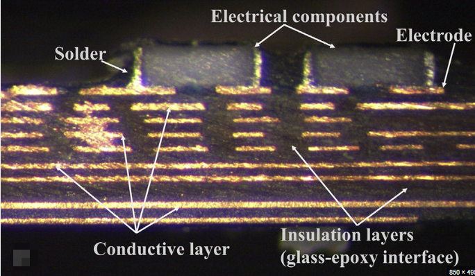
A via is a small hole in a PCB that is plated with conductive material, usually copper, to create an electrical connection between layers. Vias can vary in size, depth, and placement depending on the design needs. In mobile phones, where space is limited and signal integrity is paramount, choosing the right via type is a balancing act between manufacturability, cost, and performance. Let’s dive into the specific via types used in mobile phone PCBs and their unique benefits.
1. Through-Hole Via: The Traditional Connector
The through-hole via is the most common and oldest type of via used in PCB design. It extends through all layers of the PCB, from the top to the bottom, creating a complete pathway. In mobile phone PCBs, through-hole vias are often used for mounting components like connectors or larger chips that need strong mechanical support.
However, through-hole vias take up significant space and can interfere with high-density designs. They are also prone to signal reflection issues at high frequencies, which can impact performance in 5G-enabled devices. For instance, a poorly designed through-hole via might introduce a signal delay of up to 100 picoseconds, which is critical in high-speed applications. Because of these limitations, through-hole vias are less common in the densest areas of modern mobile phone PCBs, where smaller and more advanced vias take over.
2. Blind Via: Connecting Surface to Inner Layers
A blind via starts from the surface of the PCB (either top or bottom) and connects to an inner layer without going through the entire board. This type of via is ideal for mobile phone PCBs because it saves space on the opposite side of the board, allowing for more components or routing. Blind vias are often used to connect surface-mounted components like microchips to internal power or ground planes.
Blind vias also improve signal integrity by reducing the stub length—the unused portion of a via that can cause signal reflections. For high-frequency signals in mobile phones, such as those used in 4G or 5G communication, minimizing stub length can reduce signal loss by up to 20%. However, blind vias are more expensive to manufacture than through-hole vias due to the precision required in drilling and plating.
3. Buried Via: Hidden Connections for High Density
Buried vias are located entirely within the inner layers of a PCB, meaning they don’t reach the surface on either side. These vias are perfect for high-density interconnect (HDI) designs commonly found in mobile phones, where every millimeter of surface space counts. Buried vias allow connections between internal layers without occupying valuable real estate on the outer layers, freeing up space for additional components or traces.
In a typical mobile phone PCB with 10 layers, buried vias might connect layers 3 to 6 for power distribution while leaving the top and bottom layers free for sensitive signal routing. They also help reduce electromagnetic interference (EMI) by keeping high-speed signals confined to inner layers. However, buried vias are challenging and costly to manufacture, as they require sequential lamination during the PCB fabrication process.
4. Microvia: The Miniature Marvel for HDI Designs
Microvias are small-diameter vias, typically less than 150 micrometers, used in high-density interconnect (HDI) PCBs. They are a cornerstone of modern mobile phone designs because they enable finer pitch components and tighter routing. Microvias are usually laser-drilled, allowing for precise placement and smaller sizes compared to traditional mechanical drilling methods.
In mobile phones, microvias connect the outermost layers to the immediate inner layers, often in a stacked or staggered configuration. This reduces the board’s overall thickness and improves signal integrity for high-speed data transfer, such as in Wi-Fi or Bluetooth modules. For example, a microvia can handle signal speeds up to 10 Gbps with minimal loss, making it essential for 5G technology. The trade-off is the higher cost and complexity of manufacturing, as well as the need for advanced design software to ensure proper placement.
5. Via-in-Pad: Maximizing Space Efficiency
Via-in-pad is a specialized design technique where a via is placed directly within the pad of a surface-mounted component, such as a ball grid array (BGA) chip. This approach is widely used in mobile phone PCBs to save space and shorten signal paths. By placing the via inside the pad, designers can reduce the trace length between the component and the via, minimizing inductance and improving signal performance.
For instance, in a mobile phone’s processor chip, via-in-pad design can reduce parasitic inductance by up to 50%, ensuring faster and more reliable data transfer. However, this technique requires careful manufacturing, as the via must be filled with conductive material or capped to prevent solder wicking during assembly. Despite the added cost, via-in-pad is often the best choice for ultra-compact mobile designs where every fraction of a millimeter matters.
How Via Types Enhance Connectivity in Mobile Phones
Each via type serves a specific purpose in mobile phone PCBs, contributing to better connectivity and performance. Here’s how they work together:
- Space Optimization: Blind vias, buried vias, microvias, and via-in-pad designs allow for denser component placement, crucial in slim mobile phone designs.
- Signal Integrity: Microvias and via-in-pad reduce signal loss and interference, supporting high-speed applications like 5G and high-definition video streaming.
- Power Distribution: Through-hole and buried vias ensure stable power delivery to components across multiple layers, reducing voltage drops.
- Thermal Management: Some vias, especially through-hole vias, can also act as thermal pathways, dissipating heat from power-hungry components like processors.
By strategically combining these via types, mobile phone designers can achieve a balance of performance, cost, and manufacturability. For example, a flagship smartphone might use microvias and via-in-pad for its high-speed data circuits, while relying on buried vias for internal power planes to minimize EMI.
Challenges in Implementing Vias in Mobile Phone PCBs
While vias are essential, they come with challenges that designers must address:
- Manufacturing Complexity: Advanced vias like microvias and buried vias require precise drilling and lamination processes, increasing production costs.
- Reliability Concerns: Small vias, especially microvias, are prone to cracking under thermal stress if not designed properly, which can lead to connection failures.
- Signal Integrity Issues: Poorly placed vias can introduce impedance mismatches, causing signal reflections. For high-frequency signals, impedance mismatches as small as 5 ohms can degrade performance.
To overcome these challenges, designers must use simulation tools to model signal behavior and work closely with fabrication teams to ensure manufacturing capabilities align with design requirements.
Future Trends in Via Technology for Mobile Phones
As mobile phones continue to evolve, so does via technology. The push for thinner devices and faster connectivity is driving innovations such as:
- Stacked Microvias: Multiple microvias stacked on top of each other to connect more layers in HDI designs, allowing for even denser PCBs.
- Any-Layer Vias: Advanced laser-drilled vias that can connect any layer to any other layer, offering greater flexibility in routing.
- Conductive Fill Materials: New materials for filling vias to improve thermal conductivity and reliability, especially in high-power mobile applications.
These advancements will further enhance connectivity and performance, ensuring mobile phones keep up with demands for faster data speeds and more compact designs.
Conclusion: Choosing the Right Via for Mobile Phone PCBs
Vias are the unsung heroes of mobile phone PCBs, enabling the complex connections that power our devices. From the traditional through-hole via to the space-saving via-in-pad, each type has a specific role in enhancing connectivity, optimizing space, and ensuring signal integrity. By understanding the strengths and limitations of through-hole vias, blind vias, buried vias, microvias, and via-in-pad designs, engineers can create mobile phone PCBs that meet the demands of modern technology.
Whether you’re designing for high-speed 5G connectivity or aiming for the slimmest possible device, selecting the right via type is key. With ongoing advancements in via technology, the future of mobile phone design looks brighter—and more connected—than ever.