 ALLPCB


If you're diving into PCB design and wondering how to connect different layers of a circuit board, the answer lies in vias. Vias are small conductive paths that allow electrical signals to travel between layers of a printed circuit board (PCB). In this beginner-friendly tutorial, we'll break down everything you need to know about PCB vias, including through-hole, blind, and buried types, as well as the processes of drilling, plating, and ensuring conductivity. Whether you're new to PCB design or looking to refine your skills, this guide will make connecting layers simple and clear.
What Are PCB Vias and Why Do They Matter?
In the world of PCB design, vias are essential for creating electrical connections between different layers of a multi-layer board. A PCB often consists of multiple layers of copper foil, stacked and insulated by non-conductive materials like resin. Without vias, signals and power cannot move between these layers, making complex designs impossible.
Vias act like tiny bridges, allowing electrons to flow from one layer to another. They are critical for ensuring proper functionality, especially in compact designs where space is limited, and multiple connections are needed. Understanding how vias work and the different types available can significantly improve your PCB trace design, reduce signal loss, and enhance overall performance.
The Basics of PCB Vias: How They Work
A via is essentially a small hole drilled into a PCB that is then plated with a conductive material, usually copper, to allow electrical signals to pass through. The process starts with drilling a hole through the board or specific layers, depending on the via type. After drilling, the hole's inner surface is coated with copper through a process called electroplating. This plating ensures conductivity, enabling signals to travel between layers.
The size and placement of vias are crucial. A typical via might have a diameter of 0.2 to 0.8 mm, depending on the design requirements and manufacturing capabilities. Smaller vias save space but can be more challenging to manufacture, while larger vias are easier to produce but take up more board real estate. Proper via design also impacts signal integrity, especially in high-speed circuits where impedance mismatches can cause delays or noise. For example, a poorly designed via in a high-frequency circuit operating at 5 GHz might introduce unwanted capacitance, leading to signal degradation.
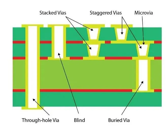
Types of PCB Vias: Through-Hole, Blind, and Buried
Not all vias are the same. Depending on your PCB design needs, you might use one of these common types: through-hole, blind, or buried vias. Each serves a specific purpose in connecting layers and optimizing space.
1. Through-Hole Vias
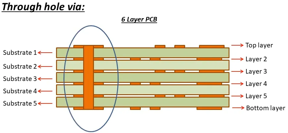
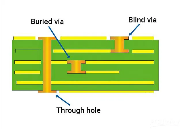
Through-hole vias are the most straightforward and widely used type. They pass through the entire thickness of the PCB, connecting the top layer to the bottom layer and any layers in between. These vias are often used in simpler designs or when components need to be mounted on both sides of the board.
Through-hole vias are easy to manufacture because they can be drilled in a single step. However, they take up space on all layers, which can be a drawback in dense, multi-layer designs. For instance, in a 4-layer PCB, a through-hole via might unnecessarily occupy space on inner layers where no connection is needed.
2. Blind Vias
Blind vias connect an outer layer of the PCB to one or more inner layers but do not pass through the entire board. For example, a blind via might connect the top layer to the second layer in a 6-layer PCB without reaching the bottom. This type of via is useful for saving space on the opposite side of the board and is often used in high-density designs.
Manufacturing blind vias is more complex than through-hole vias because they require precise drilling to a specific depth. They are typically created using laser drilling for accuracy, which can increase production costs. However, they allow for more efficient use of board space, making them ideal for compact electronics.
3. Buried Vias
Buried vias are located entirely within the inner layers of a PCB and do not connect to the outer surfaces. For instance, in an 8-layer board, a buried via might connect layers 3 and 4 without touching the top or bottom layers. These vias are perfect for very dense designs where outer layer space is at a premium.
Like blind vias, buried vias require advanced manufacturing techniques and are more expensive to produce. They are often used in complex, high-performance applications such as telecommunications or medical devices, where multiple internal connections are necessary without cluttering the surface layers.
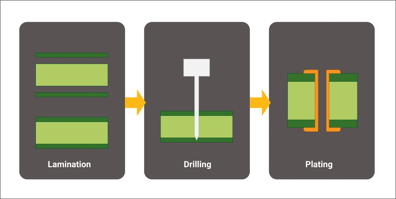
How Are PCB Vias Made? Drilling and Plating Explained
Creating vias involves two key processes: drilling and plating. These steps ensure that the vias are both structurally sound and electrically conductive.
Drilling Vias
The first step in via creation is drilling holes into the PCB. For through-hole vias, mechanical drills are commonly used, creating holes with diameters as small as 0.2 mm. For blind and buried vias, laser drilling is often preferred because it offers greater precision and can stop at specific depths.
Drilling must be done with care to avoid damaging the board or misaligning the holes. Misaligned vias can lead to poor connections or signal issues, especially in high-speed designs where even a 0.1 mm deviation can affect performance.
Plating for Conductivity
After drilling, the holes are not yet conductive because the inner surface is made of non-conductive resin or fiberglass. To make them conductive, a thin layer of copper is deposited onto the walls of the via through a process called electroplating. This copper layer, typically 0.025 mm thick, ensures that electrical signals can pass through the via with minimal resistance.
Plating is a critical step. If the copper layer is uneven or too thin, it can lead to high resistance or even open circuits. In high-current applications, insufficient plating might cause the via to overheat, potentially damaging the PCB. Manufacturers often test via conductivity to ensure it meets standards, aiming for resistances as low as a few milliohms per via.
Key Considerations for Via Design in PCB Traces
Designing vias for your PCB traces involves more than just choosing a type and drilling holes. Here are some important factors to keep in mind to ensure optimal performance and manufacturability.
1. Via Size and Aspect Ratio
The size of a via affects both its electrical performance and ease of manufacturing. Smaller vias, with diameters around 0.2 mm, are great for high-density designs but require precise drilling and plating. Larger vias, around 0.8 mm, are easier to produce but take up more space. The aspect ratio, which is the ratio of the via’s depth to its diameter, also matters. A high aspect ratio (e.g., 10:1) can make plating difficult, leading to incomplete copper coverage and poor conductivity.
2. Placement and Spacing
Vias should be placed strategically to minimize interference with other traces and components. Placing vias too close together can cause signal crosstalk, especially in high-frequency designs operating above 1 GHz. A general rule of thumb is to maintain a spacing of at least twice the via diameter between adjacent vias to avoid manufacturing issues and signal integrity problems.
3. Signal Integrity and Impedance
In high-speed circuits, vias can act as discontinuities in the signal path, introducing unwanted capacitance or inductance. For example, a via in a trace carrying a 2.5 GHz signal might add 1-2 pF of capacitance, potentially causing signal delays. To mitigate this, designers often use smaller vias or add ground vias nearby to stabilize impedance, targeting a characteristic impedance of 50 ohms for many high-speed applications.
4. Thermal and Current Handling
Vias also play a role in heat dissipation and current carrying capacity. In power circuits, larger vias or multiple vias in parallel are often used to handle higher currents, sometimes up to 2-3 amps per via, depending on the copper thickness. Thermal vias, which are specifically designed to transfer heat, can help manage temperatures in high-power components by connecting to large copper planes for heat sinking.
Common Challenges with PCB Vias and How to Avoid Them
While vias are essential, they can introduce challenges if not designed or manufactured correctly. Here are some common issues and tips to avoid them.
1. Poor Plating Leading to Open Circuits
If the copper plating inside a via is incomplete or too thin, it can result in high resistance or an open circuit. To prevent this, work with a reliable manufacturer who follows strict quality control processes. Specifying a minimum copper thickness, such as 25 micrometers, can also help ensure conductivity.
2. Via Stub Effects in High-Speed Designs
In high-speed circuits, unused portions of through-hole vias, known as stubs, can act as antennas, causing signal reflections. Using blind or buried vias instead of through-hole vias can eliminate stubs. Alternatively, back-drilling can remove the unused portion of a through-hole via, though this adds to manufacturing costs.
3. Manufacturing Limitations
Not all manufacturers can produce blind or buried vias, especially with very small diameters or high aspect ratios. Before finalizing your design, check the capabilities of your production partner. For instance, some may only support blind vias with a minimum diameter of 0.15 mm and an aspect ratio no greater than 1:1.
Beginner Tips for Using Vias in PCB Design
If you're new to PCB design, here are some practical tips to help you get started with vias and avoid common pitfalls.
- Start with through-hole vias for simpler designs. They are easier to work with and less expensive to manufacture.
- Use design software to simulate signal paths and check for potential issues like impedance mismatches before finalizing your layout.
- Keep via sizes consistent across your design to simplify manufacturing. Mixing very small and large vias can complicate the drilling process.
- Plan your layer stack-up early in the design process to decide where blind or buried vias might be needed for space efficiency.
- Always leave extra space around vias for manufacturing tolerances, especially in dense areas of the board.
Conclusion: Mastering Vias for Better PCB Designs
Vias are a fundamental part of PCB trace design, enabling the connection of multiple layers in a compact and efficient way. By understanding the differences between through-hole, blind, and buried vias, as well as the processes of drilling and plating, you can create designs that balance performance, cost, and manufacturability. Whether you're a beginner or an experienced designer, paying attention to via size, placement, and signal integrity will help you build reliable and high-performing PCBs.
With the right approach, connecting layers in your PCB can be simple and effective. Keep experimenting with via designs, and over time, you'll develop an intuition for what works best in different scenarios. Remember that every via plays a critical role in the conductivity and functionality of your board, so take the time to design them with care.


