 ALLPCB


If you're new to the world of printed circuit boards (PCBs), you might be wondering, "What are PCB layers, and why do they matter?" In simple terms, PCB layers are the different levels of conductive and insulating materials stacked together to form a circuit board. They play a critical role in how a PCB functions, affecting everything from signal speed to power distribution. Whether you're curious about PCB layer stackup explained, the difference between single layer vs double layer PCB, or the basics of multilayer PCB design for beginners, this guide will break it all down. We'll also dive into PCB layer order importance and help with understanding PCB layers from a beginner’s viewpoint.
In this blog, we'll walk you through the fundamentals of PCB layers, explain the differences between various layer types, and provide practical insights to help you grasp these concepts easily. Let’s get started on this journey to understanding how PCBs are built and why their layers are so important for electronic devices.
What Are PCB Layers?
At its core, a PCB is a flat board that connects electronic components using conductive pathways. These pathways are organized into layers, which are like thin sheets stacked on top of each other. Each layer serves a specific purpose, such as carrying signals, providing power, or grounding the circuit to prevent interference.
Think of PCB layers as floors in a building. Just as each floor in a building might have a different function (like offices on one floor and storage on another), each PCB layer has a unique role. Some layers handle electrical signals, while others manage power or reduce noise. The number of layers in a PCB can vary from just one to over a dozen, depending on the complexity of the device.
Types of PCB Layers: Single, Double, and Multilayer
PCBs come in different configurations based on the number of layers they have. Let’s explore the three main types: single-layer, double-layer, and multilayer PCBs, to help you understand their differences and uses.
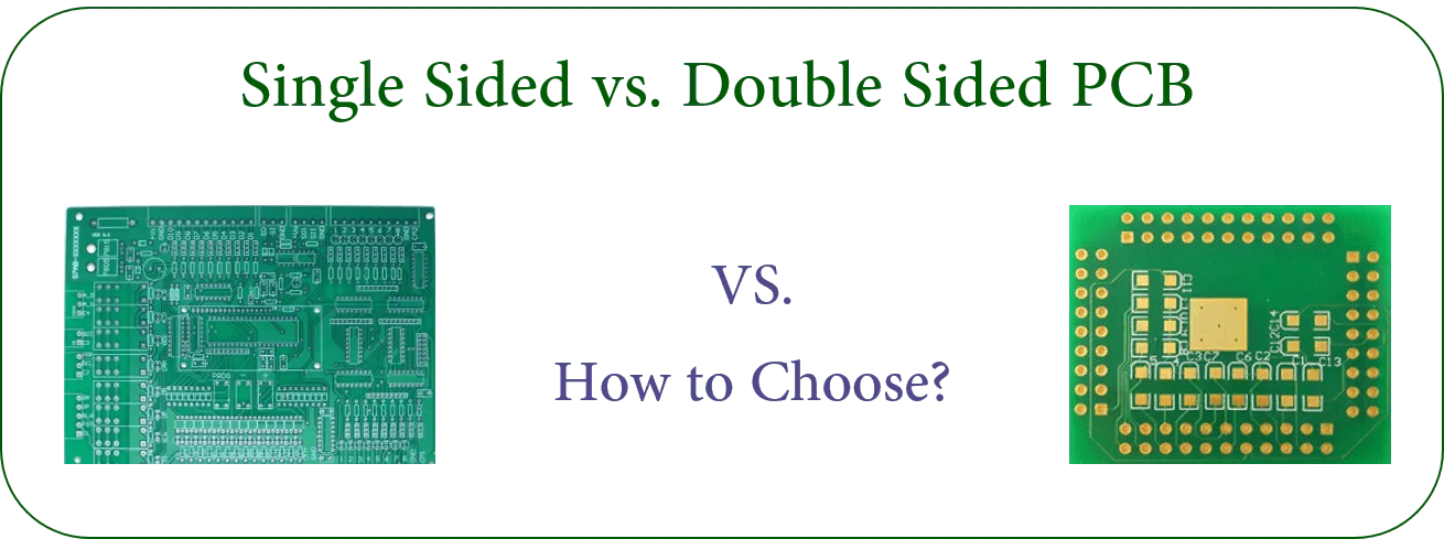
Single Layer PCBs
A single-layer PCB is the simplest type, with just one layer of conductive material (usually copper) on one side of an insulating board. These boards are easy to design and manufacture, making them cost-effective for basic projects. They’re often used in simple devices like calculators, LED lights, or basic sensors.
However, single-layer PCBs have limitations. Since there’s only one layer for routing signals, space can quickly run out for more complex circuits. This often leads to larger board sizes or the inability to support advanced features.
Double Layer PCBs
A double-layer PCB, as the name suggests, has two conductive layers—one on the top and one on the bottom of the insulating material. These layers are connected through small holes called vias, which allow signals to travel between the top and bottom. This design offers more space for routing and is ideal for slightly more complex devices like power supplies or small consumer electronics.
When comparing single layer vs double layer PCB, the double-layer option provides better flexibility and a smaller footprint since components and traces can be placed on both sides. However, it’s still limited for highly complex designs that require multiple connections.
Multilayer PCBs
For more advanced applications, multilayer PCBs come into play. These boards have three or more conductive layers sandwiched between insulating materials. The layers are connected using vias, and they often include dedicated layers for power and ground to reduce noise and improve performance.
Multilayer PCBs are used in smartphones, computers, medical devices, and other high-tech equipment. They allow for compact designs with high component density, making them a go-to choice for modern electronics. However, they are more expensive and complex to design, which is why multilayer PCB design for beginners can seem intimidating at first.
Related Reading: Optimizing 4-Layer PCB Layer Stackup: A Practical Guide
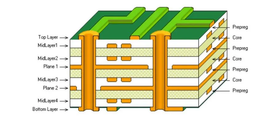
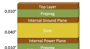
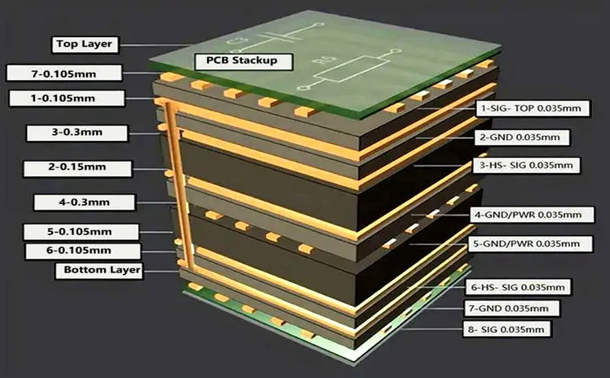
PCB Layer Stackup Explained
Now that we’ve covered the types of PCBs, let’s dive into PCB layer stackup explained in simple terms. The term "stackup" refers to the arrangement of layers in a PCB, including both conductive (copper) and insulating (dielectric) materials. A well-planned stackup ensures that the PCB performs reliably by minimizing issues like signal interference and noise.
In a typical multilayer PCB, the stackup might look like this:
- Top Layer: Used for signal routing and component placement.
- Ground Plane: A layer dedicated to grounding, which helps reduce electrical noise.
- Power Plane: A layer that distributes power to components, ensuring stable voltage levels.
- Inner Signal Layers: Additional layers for routing complex signals in dense designs.
- Bottom Layer: Similar to the top layer, used for signals and components.
Between each conductive layer, there’s an insulating material called prepreg or core, which keeps the layers separated and prevents short circuits. The thickness of these materials can vary—for example, a typical copper layer might be 0.0014 inches (1 oz of copper), while insulating layers might range from 0.005 to 0.010 inches, depending on the design requirements.
Related Reading: Decoding PCB Layer Thickness: Impact on Signal Integrity and Performance
A proper stackup design is crucial for controlling impedance, which affects how signals travel through the board. For instance, high-speed signals in a multilayer PCB might require a specific impedance value (like 50 ohms) to avoid signal loss or distortion. Poor stackup planning can lead to issues like crosstalk, where signals interfere with each other, or stray capacitance, which can slow down performance.
PCB Layer Order Importance
Understanding PCB layer order importance is key to designing a functional board. The order of layers in a PCB isn’t random—it’s carefully planned to optimize performance and minimize problems. Let’s break down why the arrangement matters.
In a multilayer PCB, ground and power planes are often placed in the middle layers. This setup helps shield signal layers from external interference and provides a stable reference for signals. For example, placing a ground plane next to a signal layer can reduce electromagnetic interference (EMI), which is critical for high-speed circuits operating at frequencies above 100 MHz.
Signal layers, on the other hand, are usually placed on the outer layers (top and bottom) for easy access during assembly and testing. However, in very complex designs, inner signal layers are also used to handle additional routing. The key is to balance the layer order so that high-speed signals are close to ground planes to maintain signal integrity.
If the layer order is incorrect, you might face issues like increased noise or poor power distribution. For instance, if a power plane is too far from the components it serves, the voltage drop could affect performance, especially in devices requiring a stable 3.3V or 5V supply.
Key Considerations for Beginners in Multilayer PCB Design
For those exploring multilayer PCB design for beginners, here are some practical tips to keep in mind when working with layers and stackups:
- Start Simple: If you’re new to PCB design, begin with a 2-layer or 4-layer board before tackling more complex multilayer designs. This will help you understand the basics of routing and layer interaction.
- Plan Your Stackup Early: Decide on the number of layers and their purpose (signal, power, ground) before starting your layout. Changing the stackup midway can lead to costly redesigns.
- Minimize Noise: Place ground planes near signal layers to reduce interference, especially for high-speed signals above 50 MHz.
- Use Vias Wisely: Vias connect layers, but too many can increase manufacturing costs and affect signal quality. Keep them to a minimum in critical areas.
- Check Impedance: For high-speed designs, ensure that your stackup supports the required impedance values (like 50 ohms for RF signals) by choosing the right materials and layer spacing.
Common Challenges When Working with PCB Layers
As a beginner, you might encounter a few hurdles when dealing with PCB layers. Here are some common challenges and how to address them:
- Signal Integrity Issues: High-speed signals can degrade if layers aren’t arranged properly. Always pair signal layers with a nearby ground plane to maintain integrity.
- Overcrowded Routing: In single or double-layer PCBs, space for traces can run out quickly. Consider moving to a multilayer design if your circuit is complex.
- Cost Constraints: Multilayer PCBs are more expensive due to additional materials and manufacturing steps. Balance performance needs with budget by optimizing the number of layers.
- Thermal Management: More layers can trap heat, especially in power-intensive designs. Use thermal vias or thicker copper layers (e.g., 2 oz instead of 1 oz) to dissipate heat.
Why Understanding PCB Layers Matters
Getting a handle on understanding PCB layers is essential for anyone stepping into electronics design. Whether you’re building a simple hobby project or working on a cutting-edge device, knowing how layers work helps you make informed decisions. A well-designed PCB with the right layer configuration ensures better performance, smaller size, and longer reliability for your product.
For instance, in a smartphone, a multilayer PCB with 8 or 10 layers allows for compact routing of high-speed data signals (up to 5 GHz in some cases) while keeping power delivery stable. Without proper layer planning, the device could suffer from dropped signals or overheating.
Conclusion
Understanding PCB layers doesn’t have to be complicated, even if you’re just starting out. From the simplicity of a single-layer board to the complexity of a multilayer design, each type of PCB serves a purpose based on the needs of your project. By grasping concepts like PCB layer stackup explained, the differences in single layer vs double layer PCB, and the essentials of multilayer PCB design for beginners, you’re already on your way to creating better circuits.
Remember the PCB layer order importance to avoid common pitfalls like noise or signal loss, and take time to plan your design carefully. With these basics under your belt, understanding PCB layers becomes a stepping stone to mastering electronics design. Keep experimenting with small projects, and soon, you’ll be confident in tackling more advanced PCB layouts.


