 ALLPCB


Are you struggling with PCB antenna issues like impedance mismatch, poor radiation patterns, tuning problems, or signal loss? You're not alone. Many engineers face these challenges when designing or troubleshooting printed circuit board (PCB) antennas. In this practical guide, we’ll dive deep into the most common PCB antenna problems and provide actionable solutions to help you achieve optimal performance. Whether you're a seasoned designer or a beginner, this blog will equip you with the tools and knowledge to tackle issues like antenna impedance mismatch, poor antenna radiation pattern, antenna tuning issues, and PCB antenna signal loss.
Why PCB Antennas Matter in Modern Design
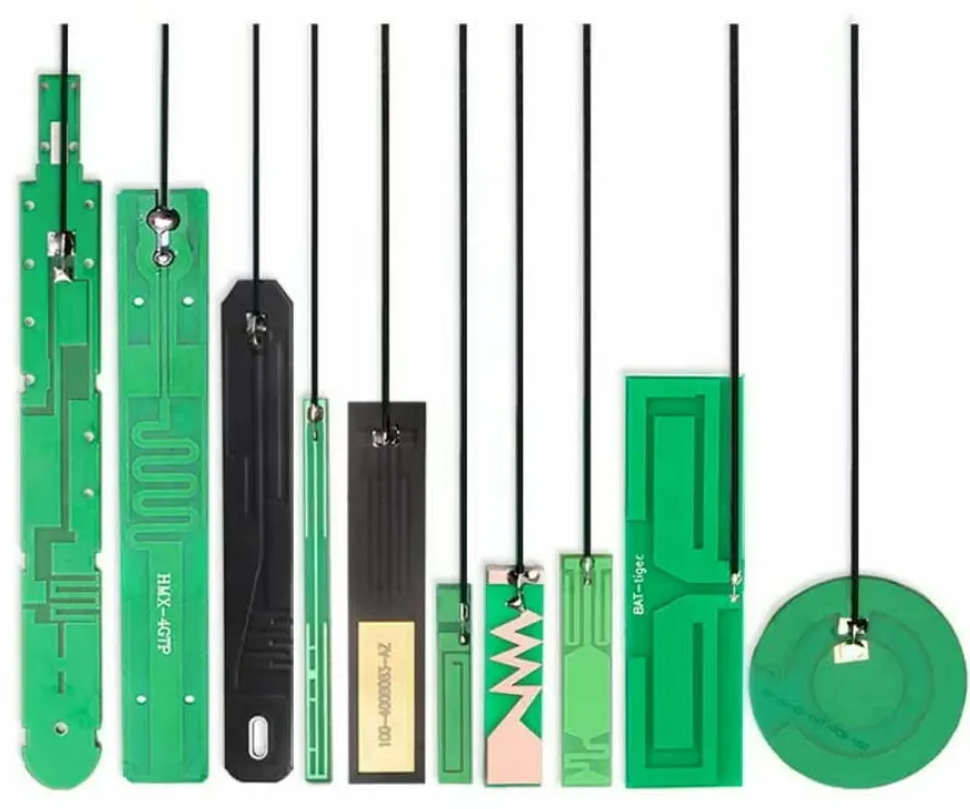
PCB antennas are a popular choice in modern electronics due to their compact size, cost-effectiveness, and ability to integrate directly into a circuit board. They are widely used in wireless devices such as smartphones, IoT modules, wearables, and more. However, their performance heavily depends on proper design, layout, and tuning. A small error can lead to significant issues like weak signal strength or complete failure of wireless communication.
In this guide, we'll break down the most common problems engineers encounter with PCB antennas and offer step-by-step solutions to fix them. Let’s get started by understanding the root causes of these issues and how to address them effectively.
Common PCB Antenna Problems and Their Symptoms
Before diving into troubleshooting, it’s essential to recognize the symptoms of PCB antenna issues. Here are the most frequent problems engineers face:
- Impedance Mismatch: Leads to signal reflection, reducing power transfer and causing poor performance.
- Poor Radiation Pattern: Results in uneven signal coverage or weak signal strength in certain directions.
- Antenna Tuning Issues: Causes the antenna to operate outside its intended frequency range, leading to inefficiency.
- Signal Loss: Manifests as reduced range or dropped connections in wireless communication.
Each of these issues can significantly impact the performance of your device. Let’s explore them in detail and provide practical solutions for PCB antenna troubleshooting.
1. Antenna Impedance Mismatch: Causes and Fixes
Impedance mismatch occurs when the antenna's impedance does not match the impedance of the connected circuit, typically 50 ohms in most RF designs. This mismatch causes signal reflections, reducing the power delivered to the antenna and degrading performance. Symptoms include high Voltage Standing Wave Ratio (VSWR) values (above 2:1) and reduced signal strength.
Common Causes of Impedance Mismatch
- Incorrect antenna dimensions or trace width, deviating from design specifications.
- Poor PCB layout, such as improper placement of ground planes or nearby components affecting impedance.
- Manufacturing variations in PCB materials or dielectric constants (e.g., FR-4 with a dielectric constant of 4.2–4.6).
Solutions for Impedance Mismatch
- Measure Impedance: Use a network analyzer to measure the antenna’s impedance and VSWR. If the impedance deviates from 50 ohms, adjustments are needed.
- Adjust Trace Dimensions: Recalculate and modify the trace width and length using impedance calculators based on your PCB stack-up and material properties.
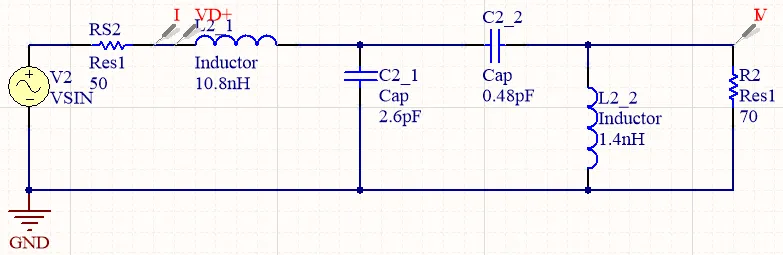
- Add Matching Components: Introduce a matching network with capacitors and inductors (e.g., a pi-network) to tune the impedance closer to 50 ohms. For instance, a 2.2 pF capacitor in parallel can often help fine-tune the match at 2.4 GHz for Wi-Fi applications.
- Optimize Ground Plane: Ensure the ground plane under the antenna is continuous and free from cuts or nearby traces that could alter impedance.
2. Poor Antenna Radiation Pattern: Identifying and Resolving Issues
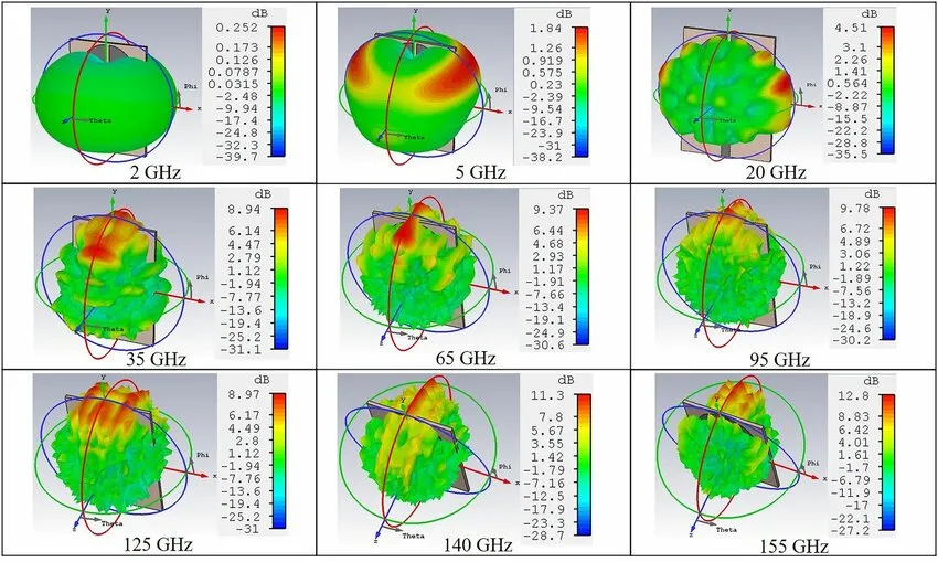
A poor antenna radiation pattern means the antenna does not radiate energy evenly or in the desired direction. This can lead to weak signals in critical areas or interference in unintended directions. For example, a monopole PCB antenna might show a distorted omnidirectional pattern if placed too close to metallic components.
Common Causes of Poor Radiation Patterns
- Obstructions or nearby components (e.g., metal enclosures or large capacitors) interfering with the antenna’s field.
- Incorrect antenna placement on the PCB, such as near the edge or center without proper clearance.
- Ground plane issues, like an undersized or improperly shaped ground plane affecting the radiation pattern.
Solutions for Poor Radiation Patterns
- Simulate the Pattern: Use electromagnetic simulation tools to visualize the radiation pattern. Look for nulls or distortions in the pattern that indicate issues.
- Reposition the Antenna: Place the antenna at the edge of the PCB with a clear area around it (at least 5–10 mm) to avoid interference from components or enclosures.
- Optimize Ground Plane Size: Ensure the ground plane extends at least a quarter-wavelength (e.g., 31 mm for 2.4 GHz) beyond the antenna for better radiation efficiency.
- Use Shielding: If nearby components are unavoidable, add shielding cans to minimize interference with the antenna’s field.
3. Antenna Tuning Issues: How to Get the Frequency Right
Antenna tuning issues arise when the antenna does not resonate at the intended frequency, such as 2.4 GHz for Bluetooth or Wi-Fi. This results in reduced efficiency and poor signal strength. You might notice this as a shifted resonant frequency when testing with a spectrum analyzer.
Common Causes of Tuning Problems
- Inaccurate antenna dimensions due to design or manufacturing errors.
- Variations in PCB material properties, affecting the effective dielectric constant and thus the resonant frequency.
- Environmental factors, such as nearby plastics or metals detuning the antenna after assembly.
Solutions for Antenna Tuning Issues
- Measure Resonant Frequency: Use a vector network analyzer to check the antenna’s S11 parameter (return loss). A dip in the S11 graph should align with your target frequency (e.g., -10 dB or lower at 2.4 GHz).
- Adjust Antenna Length: If the resonant frequency is too high, slightly increase the antenna length (e.g., by 1–2 mm). If too low, trim it down. For a 2.4 GHz inverted-F antenna, the length should be approximately 31 mm (quarter-wavelength).
- Use Tuning Components: Add small capacitors or inductors near the antenna feed to shift the resonant frequency. A 1 pF capacitor can often lower the frequency slightly.
- Account for Enclosure Effects: Test the antenna after assembly in its final enclosure, as materials like plastic can shift the frequency by 1–2%.
4. PCB Antenna Signal Loss: Diagnosing and Reducing Losses
Signal loss in PCB antennas results in reduced communication range and unreliable connections. It can stem from various factors, including inefficiencies in the antenna design, PCB material losses, or external interference. You might measure this as a low received signal strength indicator (RSSI) value, such as below -80 dBm in a wireless system.
Common Causes of Signal Loss
- High dielectric losses in PCB materials, especially in low-cost substrates like FR-4 at frequencies above 2 GHz.
- Parasitic effects from nearby traces or components absorbing or scattering the signal.
- Improper feedline design, causing additional losses before the signal reaches the antenna.
Solutions for Reducing Signal Loss
- Choose the Right Material: For high-frequency applications (above 2 GHz), consider low-loss materials with a loss tangent below 0.005, as opposed to standard FR-4 with a loss tangent of 0.02.
- Minimize Feedline Length: Keep the RF feedline as short as possible to reduce transmission line losses. Use a 50-ohm microstrip or coplanar waveguide design for the feedline.
- Isolate the Antenna: Ensure no high-speed digital traces or noisy components are near the antenna to avoid parasitic coupling and signal absorption.
- Test in Real Conditions: Measure signal strength in the intended operating environment to account for external factors like interference or multipath effects.
Best Practices for Preventing PCB Antenna Problems
While troubleshooting is essential, preventing issues during the design phase can save time and resources. Here are some best practices to ensure your PCB antenna performs optimally from the start:
- Follow Design Guidelines: Adhere to antenna design rules specific to your frequency band, such as quarter-wavelength dimensions (e.g., 31 mm for 2.4 GHz).
- Simulate Before Fabrication: Use RF simulation software to predict impedance, radiation patterns, and resonant frequency before manufacturing.
- Prototype and Test: Build prototypes and test them with proper equipment like network analyzers to catch issues early.
- Maintain Clear Documentation: Document your design parameters, material choices, and test results to streamline troubleshooting if problems arise.
Tools for Effective PCB Antenna Troubleshooting
Having the right tools can make PCB antenna troubleshooting much easier. Here are some essential tools and their uses:
- Vector Network Analyzer (VNA): Measures impedance, VSWR, and return loss for diagnosing mismatch and tuning issues.
- Spectrum Analyzer: Helps identify signal strength and interference in the operating frequency band.
- Electromagnetic Simulation Software: Simulates radiation patterns and predicts performance before fabrication.
- Oscilloscope: Useful for checking signal integrity at the antenna feed point.
Conclusion: Mastering PCB Antenna Troubleshooting
Troubleshooting PCB antenna problems like impedance mismatch, poor radiation patterns, tuning issues, and signal loss can be challenging, but with the right approach, you can achieve reliable performance. By understanding the root causes of these issues—whether it’s a mismatched 50-ohm impedance, a distorted radiation pattern due to placement, or detuning from environmental factors—you can apply targeted solutions to fix them.
Remember to measure and test at every stage, from design to final assembly, using tools like network analyzers and simulation software. Incorporate best practices during the design phase to prevent issues before they occur. With this practical guide, you’re well-equipped to tackle PCB antenna troubleshooting and optimize your wireless designs for success.
At ALLPCB, we’re committed to supporting engineers with resources and expertise to bring their designs to life. Whether you’re facing challenges with antenna performance or other PCB design aspects, we’re here to help you achieve your goals with high-quality manufacturing and assembly services.


