 ALLPCB


When it comes to PCB assembly, choosing the right stencil can make or break the quality of your final product. If you're wondering whether a step stencil or a standard stencil is the best fit for your project, you're in the right place. In short, standard stencils work well for simpler designs with uniform component sizes, while step stencils are ideal for complex boards with varying component heights and solder paste requirements. This blog will dive deep into the differences, exploring step stencil advantages, standard stencil limitations, and providing a stencil selection guide to help you make an informed decision. We'll also cover a cost comparison to ensure you get the best value for your PCB assembly needs.
Understanding PCB Stencils: Why They Matter in Assembly
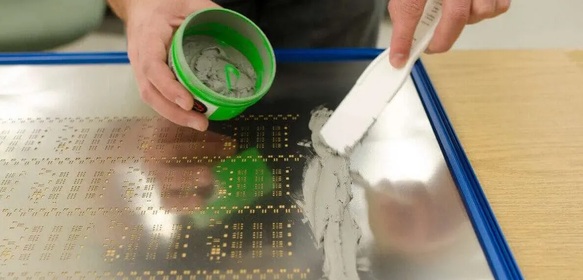
In the world of surface mount technology (SMT), stencils are essential tools for applying solder paste to printed circuit boards (PCBs). These thin sheets, usually made of stainless steel, have precise openings that align with the PCB's pads. During assembly, solder paste is pushed through these openings, ensuring accurate placement for components before soldering.
Choosing the right stencil directly impacts the quality of solder joints, the reliability of the final product, and even the efficiency of the assembly process. A mismatch between your stencil and project needs can lead to issues like insufficient solder, bridging, or defective connections. With modern electronics becoming smaller and more complex, understanding the differences between standard and step stencils is more important than ever.
What is a Standard Stencil?
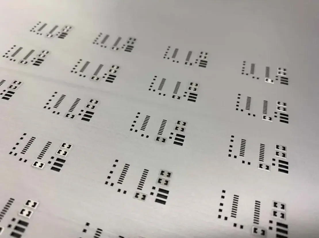
A standard stencil, also known as a flat stencil, is a single-thickness sheet of metal with laser-cut openings for solder paste deposition. It’s the most common type of stencil used in PCB assembly due to its simplicity and affordability. Standard stencils are typically between 0.1 mm and 0.15 mm thick, depending on the component sizes and pitch (distance between pins) on the PCB.
These stencils are designed for boards where components have similar solder paste volume requirements. They work best with designs that don’t have a mix of very small and very large components. For example, a board with mostly 0603 resistors and capacitors (1.6 mm x 0.8 mm) can often be assembled effectively using a standard stencil with uniform thickness.
Advantages of Standard Stencils
- Cost-Effective: Standard stencils are generally cheaper to manufacture since they don’t require additional processing for varying thicknesses.
- Simplicity: They are straightforward to design and use, making them ideal for less complex PCB layouts.
- Wide Availability: Most assembly houses and manufacturers offer standard stencils as a default option, ensuring quick turnaround times.
Standard Stencil Limitations
While standard stencils are practical for many projects, they come with notable limitations, especially for modern, high-density boards:
- Uniform Solder Volume: They deposit the same amount of solder paste across the board, which can be problematic for mixed-component designs. For instance, fine-pitch components (like 0.4 mm pitch QFNs) need less paste, while larger connectors may require more, leading to potential defects.
- Limited Flexibility: They struggle with boards that have components of varying heights or sizes, often resulting in inconsistent soldering quality.
- Higher Risk of Defects: Without adjustments in thickness, there’s a greater chance of issues like solder bridging on fine-pitch components or insufficient paste for larger parts.
What is a Step Stencil?
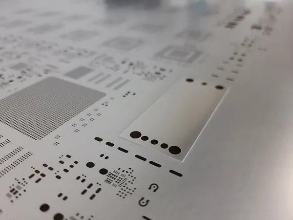
A step stencil is a more advanced option designed to address the challenges of complex PCB designs. Unlike a standard stencil, a step stencil has varying thicknesses across its surface. These variations, created through processes like milling or chemical etching, form “step-up” areas (thicker regions) and “step-down” areas (thinner regions) to control the amount of solder paste deposited on different parts of the board.
For example, a step-down area of 0.08 mm thickness might be used for fine-pitch components like 0402 capacitors (1.0 mm x 0.5 mm), while a step-up area of 0.2 mm could cater to larger components like power connectors. This customization ensures optimal solder paste volume for each component type, improving assembly quality.
Step Stencil Advantages
Step stencils offer several benefits that make them a go-to choice for intricate PCB assembly projects:
- Precision in Solder Paste Volume: By varying thickness, step stencils deliver the right amount of paste for each component, reducing defects. For instance, a fine-pitch IC with a 0.5 mm pitch might need only 0.05 cubic mm of paste per pad, while a large connector could require 0.2 cubic mm—step stencils make this possible in one pass.
- Versatility: They handle mixed-component boards with ease, accommodating everything from tiny chip resistors to large through-hole parts on the same PCB.
- Improved Quality: With tailored paste deposition, the risk of issues like bridging or insufficient solder drops significantly, leading to higher first-pass yields in assembly.
- Supports High-Density Designs: As electronics shrink, step stencils are better suited for densely packed boards with fine-pitch components (below 0.5 mm).
Limitations of Step Stencils
Despite their advantages, step stencils aren’t without drawbacks:
- Higher Cost: The manufacturing process for step stencils is more complex, involving additional steps like milling or etching, which increases production costs.
- Longer Lead Times: Due to the customized nature of step stencils, they often take longer to produce compared to standard stencils.
- Design Complexity: Creating a step stencil requires precise planning and coordination with the PCB design to ensure the step areas align perfectly with component needs.
Stencil Selection Guide: Step Stencil vs. Standard Stencil
Deciding between a step stencil and a standard stencil depends on several factors related to your PCB design and assembly goals. Use this stencil selection guide to determine which option suits your project best.
1. Component Types and Sizes
- Standard Stencil: Choose this if your board has components of similar sizes and solder paste needs, such as a design dominated by 0805 or 0603 passives. It’s sufficient for pitches above 0.8 mm.
- Step Stencil: Opt for this if your board mixes fine-pitch components (below 0.5 mm) with larger parts like connectors or power modules. It’s ideal for high-density designs with diverse requirements.
2. Board Complexity
- Standard Stencil: Best for simpler, low-to-medium density boards where uniform paste application won’t cause issues.
- Step Stencil: Necessary for complex, high-density boards where precise control over solder paste volume is critical to avoid defects.
3. Production Volume
- Standard Stencil: Suitable for low-volume or prototype runs where cost savings are a priority and minor defects can be manually corrected.
- Step Stencil: Recommended for high-volume production where consistency and high first-pass yield are essential to minimize rework costs.
4. Budget Constraints
- Standard Stencil: A better fit if you’re working with a tight budget and your design doesn’t demand advanced stencil features.
- Step Stencil: Worth the investment if quality and reliability are non-negotiable, especially for commercial or critical applications.
Cost Comparison: Step Stencil vs. Standard Stencil
Cost is often a deciding factor in PCB assembly, and understanding the financial implications of your stencil choice is crucial. Here’s a detailed cost comparison to help you weigh the options.
Manufacturing Costs
Standard stencils are typically less expensive to produce because they involve a straightforward laser-cutting process with no additional customization. On average, a standard stencil for a small to medium-sized PCB might cost between $50 and $150, depending on the size and material.
Step stencils, on the other hand, require more intricate manufacturing techniques, such as milling or chemical etching, to create varying thicknesses. This added complexity can drive the cost to $200–$500 or more for a similar-sized stencil. The exact price depends on the number of step areas and the precision required.
Assembly Efficiency and Yield
While standard stencils have a lower upfront cost, they can lead to higher expenses during assembly if defects occur. For instance, inconsistent solder paste application might result in a 10–20% defect rate on complex boards, requiring rework or scrap, which adds labor and material costs.
Step stencils, though pricier initially, often improve first-pass yield to 95% or higher by minimizing defects. This efficiency can save significant costs in high-volume production, where even a 1% reduction in defects translates to hundreds or thousands of dollars saved.
Long-Term Value
For low-volume or prototype projects, the cost savings of a standard stencil usually outweigh the benefits of a step stencil. However, for large-scale production or designs with strict quality requirements, the investment in a step stencil pays off through reduced rework and higher reliability.
Practical Tips for Choosing and Using Stencils in PCB Assembly
Beyond selecting the right stencil type, proper usage and maintenance are key to achieving optimal results in PCB assembly. Here are some actionable tips to ensure success:
- Work Closely with Your Manufacturer: Provide detailed design files and component specifications to ensure the stencil openings and thicknesses match your board’s needs.
- Consider Stencil Thickness Early: For standard stencils, a thickness of 0.12 mm is a common starting point for pitches between 0.65 mm and 1.0 mm. For step stencils, consult with your assembly team to determine step-up and step-down values based on component datasheets.
- Maintain Stencil Cleanliness: Residue from solder paste can clog openings, leading to uneven application. Clean the stencil after every 5–10 prints using isopropyl alcohol and a lint-free cloth.
- Inspect Regularly: Check for wear or damage to the stencil, especially in high-volume runs. A worn stencil can cause misalignment or inconsistent paste deposition.
- Test with Prototypes: Before committing to full production, run a small batch to verify that the stencil performs as expected with your specific PCB design.
Conclusion: Making the Right Choice for Your PCB Project
Selecting between a step stencil and a standard stencil boils down to the specific needs of your PCB assembly project. If your design is straightforward with uniform components and you’re focused on keeping costs low, a standard stencil is likely the way to go. However, if you’re dealing with a complex, high-density board that mixes fine-pitch and larger components, the step stencil advantages—such as precise solder paste control and improved quality—make it a worthy investment despite the higher cost.
By using this stencil selection guide and considering factors like component types, board complexity, production volume, and budget, you can confidently choose the best option for your needs. Remember that the right stencil not only enhances assembly quality but also saves time and resources in the long run. Whether you prioritize cost savings or top-tier performance, understanding the strengths and limitations of each stencil type ensures your PCB project succeeds from design to delivery.


