 ALLPCB


Are you a hobbyist looking to design a multi-layer PCB but worried about the complexity of Design for Manufacturability (DFM)? Don’t stress! Multi-layer PCB DFM can be simplified with the right approach, tools, and tips. In this beginner’s guide, we’ll break down the essentials of PCB design for beginners, focusing on hobbyist PCB DFM, easy PCB design, low-cost PCB options, and simple PCB manufacturing techniques. Whether you’re building a small project or prototyping an idea, this guide will help you create reliable multi-layer PCBs without breaking the bank or getting overwhelmed.
Let’s dive into the world of multi-layer PCBs and explore how to make the process straightforward and accessible, even if you’re just starting out.
What Is a Multi-Layer PCB and Why Use It?
A multi-layer PCB (Printed Circuit Board) is a circuit board with more than two layers of conductive copper, separated by insulating materials. Unlike single- or double-layer boards, multi-layer PCBs can have 4, 6, 8, or even more layers, making them ideal for complex designs that require compact layouts and high performance.
For hobbyists, multi-layer PCBs might seem like overkill for simple projects, but they offer several benefits:
- Space Efficiency: They allow you to pack more components into a smaller area, which is great for compact devices.
- Better Signal Integrity: With dedicated ground and power planes, multi-layer boards reduce noise and interference, crucial for high-speed signals (e.g., above 50 MHz).
- Improved Routing: More layers mean more room to route traces, avoiding cross-talk and signal delays.
However, designing multi-layer PCBs comes with challenges, especially when it comes to manufacturability. That’s where DFM (Design for Manufacturability) steps in. DFM ensures your design can be easily and affordably produced without errors. For hobbyists, mastering hobbyist PCB DFM is key to creating low-cost PCBs without sacrificing quality.
Understanding Hobbyist PCB DFM: Why It Matters
Design for Manufacturability (DFM) is the process of designing your PCB in a way that makes it easy and cost-effective to manufacture. For hobbyists, focusing on hobbyist PCB DFM means avoiding common pitfalls that can lead to delays, extra costs, or failed boards.
Here are some reasons why DFM is critical for beginners working on multi-layer PCBs:
- Cost Control: Poor design choices, like overly tight tolerances (e.g., trace widths below 6 mils), can increase manufacturing costs or lead to rejected boards.
- Production Reliability: Following DFM guidelines reduces the chance of errors like short circuits or misaligned layers during fabrication.
- Time Efficiency: A DFM-friendly design speeds up the manufacturing process since there’s less back-and-forth with the fabricator to fix issues.
As a hobbyist, your goal is to keep things simple and affordable. By applying DFM principles tailored to multi-layer PCBs, you can achieve easy PCB design and ensure simple PCB manufacturing, even on a tight budget.
Key Steps to Simplify Multi-Layer PCB Design for Beginners
Designing a multi-layer PCB doesn’t have to be intimidating. By breaking it down into manageable steps and focusing on DFM, you can create a functional board without unnecessary stress. Let’s walk through the essentials of PCB design for beginners.
1. Start with a Clear Schematic
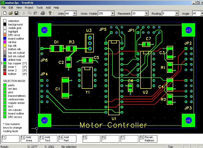
Before jumping into the layout, create a detailed schematic. This is the blueprint of your circuit, showing how components connect. Use design software that supports multi-layer boards and has built-in DFM checks. A clear schematic helps prevent errors in the layout stage and ensures you don’t miss critical connections.
Tip: Group related components (e.g., power supply parts) together in the schematic to make routing easier later. Double-check for errors like unconnected pins or incorrect component values (e.g., using a 1kΩ resistor instead of 10kΩ).
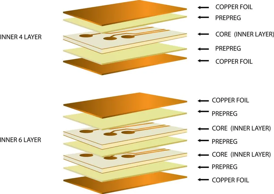
2. Plan Your Layer Stack-Up
The layer stack-up defines the arrangement of copper and insulating layers in your multi-layer PCB. For hobbyists, a 4-layer board is often a good starting point. A common 4-layer stack-up looks like this:
- Top Layer: Signal traces and components.
- Inner Layer 1: Ground plane to reduce noise.
- Inner Layer 2: Power plane for stable voltage distribution.
- Bottom Layer: Additional signal traces or components.
Planning your stack-up with DFM in mind means keeping signal layers close to ground planes to minimize electromagnetic interference (EMI). For high-speed designs, ensure that signal traces don’t cross splits in ground planes, as this can cause signal integrity issues.
Tip: Stick to standard layer counts (e.g., 4 or 6 layers) to keep costs down. Odd-numbered layers or non-standard configurations can increase manufacturing expenses by 20-30%.
3. Follow Basic Design Rules for Easy PCB Design
Every PCB manufacturer has design rules that specify minimum trace widths, spacing, and other parameters. Following these rules is a cornerstone of hobbyist PCB DFM. Here are some beginner-friendly guidelines for multi-layer designs:
- Trace Width and Spacing: Use a minimum trace width of 6-8 mils (0.15-0.2 mm) and spacing of 6 mils for most designs to avoid manufacturing issues.
- Via Size: Keep via drill sizes at or above 12 mils (0.3 mm) to ensure reliability during drilling.
- Clearance: Maintain at least 10 mils (0.25 mm) clearance between traces and board edges to prevent damage during fabrication.
Many design tools have built-in Design Rule Check (DRC) features that alert you to violations. Run these checks often to catch issues early.
4. Optimize Component Placement
Place components logically to minimize trace lengths and reduce interference. For multi-layer PCBs, group high-speed components (e.g., microcontrollers running at 100 MHz) near their related circuits to avoid long traces that can degrade signal quality.
Tip: Place decoupling capacitors (e.g., 0.1 μF) close to power pins of ICs to stabilize voltage and reduce noise. A distance of less than 100 mils (2.54 mm) is ideal.
5. Route Traces with Care
Routing is where multi-layer PCBs shine, as you have more layers to work with. However, poor routing can lead to signal issues or manufacturing defects. Follow these DFM tips for routing:
- Avoid 90-Degree Angles: Use 45-degree angles or curves to reduce signal reflection and improve manufacturability.
- Minimize Via Usage: Excessive vias can increase costs and introduce weak points. Aim for fewer than 10 vias per square inch if possible.
- Separate High-Speed and Low-Speed Signals: Route high-speed traces (e.g., USB or HDMI signals at 480 Mbps) on different layers from low-speed ones to avoid interference.
Low-Cost PCB Strategies for Hobbyists
One of the biggest concerns for hobbyists is keeping costs down. Multi-layer PCBs are inherently more expensive than single-layer boards, but with smart choices, you can achieve low-cost PCB designs without compromising quality. Here’s how:
1. Stick to Standard Specifications
Manufacturers offer the best pricing for standard board sizes, thicknesses, and materials. For example:
- Board Thickness: Use a standard thickness of 1.6 mm for most multi-layer boards.
- Board Size: Keep your design within common panel sizes (e.g., under 100 mm x 100 mm) to avoid extra fees.
- Material: Choose FR-4, the most common and affordable PCB material, with a dielectric constant of around 4.5 at 1 MHz.
Non-standard specs can increase costs by 50% or more, so always check the manufacturer’s capabilities and pricing before finalizing your design.
2. Order in Bulk for Discounts
Even as a hobbyist, ordering multiple copies of your PCB can lower the per-unit cost. For instance, ordering 10 boards instead of 1 might reduce the price per board from $5 to $2, depending on the service provider.
3. Use Free or Low-Cost Design Tools
Many design software options offer free versions with features suitable for hobbyist PCB DFM. These tools often include libraries of components, simulation capabilities, and DFM rule checks to help you design low-cost PCBs without expensive software subscriptions.
Simple PCB Manufacturing: Preparing Your Design for Production
Once your design is complete, the next step is manufacturing. Simple PCB manufacturing starts with preparing your files correctly to avoid delays or errors. Here’s how to ensure a smooth process:
1. Generate Gerber Files
Gerber files are the standard format for PCB manufacturing. They include all the details of your design, such as copper layers, solder mask, and drill holes. Most design software can export these files. Double-check that each layer (e.g., top copper, bottom copper) is correctly labeled and included.
2. Include a Bill of Materials (BOM)
A BOM lists all components in your design, including part numbers, quantities, and descriptions. This helps the manufacturer or assembler source the right parts if you’re opting for assembly services.
3. Run a Final DFM Check
Before submitting your files, run a final DFM check using your software or an online tool provided by many manufacturers. This ensures your design meets all manufacturing requirements, such as minimum trace widths or via sizes.
Common Mistakes to Avoid in Multi-Layer PCB Design
Even with the best intentions, beginners often make mistakes that can derail their projects. Here are some common pitfalls in multi-layer PCB design and how to avoid them:
- Ignoring Ground Planes: Skipping a dedicated ground plane can lead to noise issues, especially in high-speed designs. Always allocate at least one layer for grounding.
- Overcomplicating the Design: Adding too many layers (e.g., 8 layers for a simple project) increases costs unnecessarily. Stick to the minimum layers needed.
- Forgetting Thermal Management: High-power components generate heat. Place thermal vias (e.g., 0.3 mm diameter, spaced 1 mm apart) near these components to dissipate heat to inner layers.
Final Thoughts on Multi-Layer PCB DFM for Hobbyists
Designing a multi-layer PCB as a hobbyist may seem daunting at first, but with the right mindset and tools, it’s entirely achievable. By focusing on hobbyist PCB DFM, you can create easy PCB designs that are ready for simple PCB manufacturing while keeping costs low. Start with a clear schematic, plan your layer stack-up, follow basic design rules, and always double-check your work with DFM tools.
Remember, the key to success in PCB design for beginners is to start small, learn from each project, and refine your skills over time. With these tips and strategies, you’re well on your way to building reliable, low-cost PCBs for your hobby projects. Let’s turn your ideas into reality with confidence!


