ALLPCB


Overview
Consumers expect long battery life from earbuds, wearables, and other ultra-compact electronic products despite small form factors. Device size limits battery capacity. This article describes how single-inductor, multiple-output (SIMO) switch-mode regulator architectures can save board space. The SIMO architecture and low quiescent current of these regulators help extend battery life in space-constrained electronic products.
Purpose of this article
This article explains SIMO technology and how it works. It also describes power-management ICs (PMICs) that use SIMO regulators to reduce power consumption and overall component count while providing comparable functionality to conventional solutions in less than half the footprint.
Introduction
Meeting battery life requirements for miniature devices
When you wear earbuds for long hikes or work on a large project all afternoon, you do not want to interrupt the activity to recharge. You expect earbuds, wearables, and other small battery-powered electronics to operate reliably for extended periods.
From a design perspective this is challenging. Size constraints drive the use of small Li+ batteries, which must last long between charges and be used efficiently. The power system must also satisfy a variety of subsystem voltage requirements.
The SIMO architecture addresses these systems by integrating functions that would otherwise require multiple discrete components. The following sections examine SIMO and its suitability for buck-boost regulators.
SIMO architecture overview
In conventional switch-mode regulator topologies, each regulator typically requires a separate inductor for each output rail, because each voltage rail must be served by its own inductor (see Figure 1). Inductors are large and costly, which is a drawback for small products. Linear regulators offer an alternative: they are compact and low-noise but suffer efficiency loss. A hybrid approach uses multiple low-dropout regulators (LDOs) with DC-DC converters, but that configuration still increases power dissipation and board area compared with a single integrated solution.
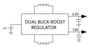
Figure 1. Conventional buck-boost switch regulator architecture.
Selected buck-boost SIMO converters can regulate up to three output voltages over a wide output range using a single inductor. The buck-boost topology makes better use of the inductor because, compared with buck-only SIMO, it spends less time maintaining each channel. Buck-only SIMO weaknesses are amplified when one or more outputs approach the input voltage. When an output voltage nears the battery voltage, a buck-only SIMO requires the inductor to spend excessive time on that channel, degrading others.
Sometimes the system requires an inductor. LDOs can never provide boost capability. Because SIMO requires only one inductor, a buck-boost SIMO is generally preferable when at least one boost output is needed.
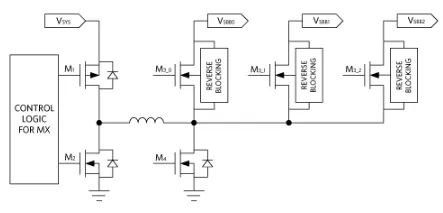
Figure 2. SIMO architecture block diagram.
Inductor saturation current (Isat) measures the current level at which inductance drops to a specified percentage and is proportional to core material and size. Using a single inductor in a SIMO architecture offers several advantages over multiple independent DC-DC converters:
- Better utilization of available Z height when the system allows.
- Reduced number of inductors compared with traditional solutions, saving cost and board area.
- Time multiplexing, which is effective when different functions are not usually active simultaneously. This advantage appears when total supply current is less than the sum of individual output currents. For example, different voltage rails may be required sequentially during operation. In some Bluetooth systems, data may be downloaded before enabling a function. The radio-related supply and the function enable time differ, so the required total Isat for the SIMO inductor is lower than the sum required by separate converters.
RMS current rating of the inductor also benefits the SIMO approach, since peak power events across channels usually do not coincide, lowering the inductor's total RMS requirement even if channels are not time-multiplexed.
Trade-offs and mitigation
Using SIMO involves trade-offs that require careful design. Output voltage ripple tends to be higher because a single inductor feeds multiple outputs alternately. Heavy SIMO loading with time multiplexing and delayed service intervals for each channel can further increase output ripple. Larger output capacitors can mitigate ripple while preserving footprint and BOM advantages.
Maxim's PMICs MAX77650 and MAX77651 implement a micro-power SIMO buck-boost DC-DC converter design that balances these trade-offs. These PMICs integrate 150 mA LDOs to provide ripple suppression for noise-sensitive applications such as audio. Optional series resistors (24 Ω) on the serial data (SDA) and serial clock (SCL) lines reduce bus crosstalk and undershoot, while protecting device inputs from high-voltage spikes on the bus. Each regulator module has low quiescent current (1 μA per output), helping extend battery life. The ICs operate in discontinuous conduction mode (DCM), so inductor current returns to zero each cycle to reduce crosstalk and prevent oscillation.
SIMO converters take advantage of the full battery voltage range since each output in a buck-boost configuration can be above, below, or equal to the input. Peak inductor current is programmable, allowing optimization of efficiency, output ripple, electromagnetic interference (EMI), PCB layout, and load capability. These ICs achieve better than 85% efficiency at a 3.3 V output.
This SIMO architecture provides a balance between low power consumption and compact size, which is important for very small applications with limited heat dissipation. Figure 3 compares the MAX77650 PMIC with solutions using multiple LDOs or multiple DC-DC converters in terms of heat dissipation and footprint.
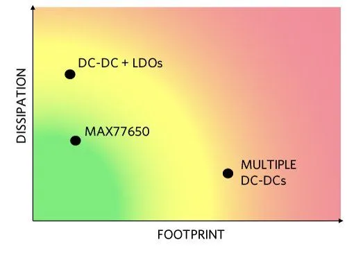
Figure 3. MAX77650 PMIC shows low thermal dissipation and small footprint for space-constrained battery-powered devices such as earbuds and wearables.
The SIMO control scheme in MAX77650/1 uses a proprietary controller to ensure timely servicing of all outputs. If no regulator needs servicing, the state machine stays in low-power mode. When the controller detects a regulator requires servicing, it charges the inductor until the peak current limit is reached, then discharges the inductor into the corresponding output until the current reaches zero. If multiple outputs need servicing simultaneously, the controller ensures no single output occupies all switching cycles; instead, cycles are interleaved among the outputs that require service, skipping outputs that do not need service.
The SIMO architecture also provides soft-start to minimize inrush current by limiting the slew rate of output voltages during startup. Each SIMO buck-boost channel includes an active discharge feature that automatically enables per-channel discharge based on the SIMO regulator state to fully and promptly power down system peripherals. Active discharge can also be controlled via I2C.
Power performance: SIMO vs conventional architectures
Figure 4 shows a possible power-tree diagram using the MAX77650. Three of four loads are connected to the Li+ battery through the efficient SIMO switch regulator; the fourth load is powered by an LDO from a 2.05 V SIMO output with 90.2% efficiency (1.85 V/2.05 V). Table 1 compares power performance between the conventional architecture and a SIMO-based architecture.
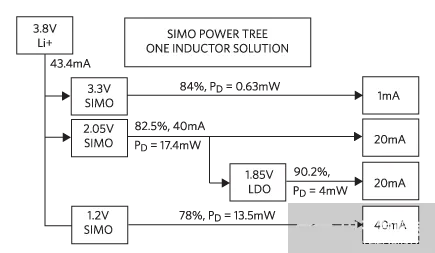
Figure 4. Example power tree using the MAX77650 PMIC for space-constrained battery-powered devices.
| Parameter | Conventional solution | SIMO | SIMO advantage |
| Li+ battery current | 49 mA | 43.5 mA | SIMO saves 5.6 mA |
| System efficiency | 69.5% | 78.4% | SIMO improves efficiency by 8.9% |
| Minimum Li+ battery voltage | 3.4 V (due to 3.3 V LDO) | 2.7 V | SIMO allows deeper discharge |
Design considerations and calculator tool
A SIMO calculator can help explore trade-offs related to SIMO parameters. The SIMO output voltage ripple depends on output capacitors, the inductor, output voltage settings, and peak current limit settings. Available SIMO output current depends on input voltage, output voltage, peak current limit, and currents drawn by other SIMO channels. SIMO switching frequency depends on input voltage, output voltage, peak current limit, and the inductor.
In the spreadsheet-based calculator, enter system parameters into the appropriate cells at the top of each row. Key computed values are highlighted. Cells outside normal operating ranges are flagged, and notes provide guidance for improving the design.
Conclusion
For earbuds, wearables, and similar small battery-powered electronics, extended battery life is critical for customer satisfaction. Compared with conventional buck-boost topologies, SIMO architectures reduce component count and typically extend battery life. This article reviewed PMICs that integrate SIMO switch regulators and are well suited to the challenges of ultra-low-power, space-constrained applications.