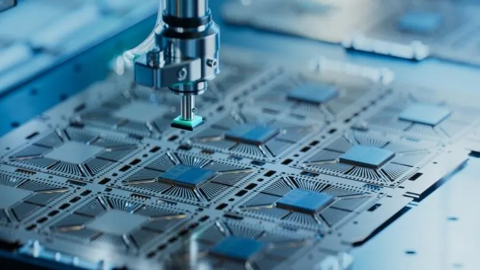
ALLPCB


This article analyzes modern electronic integration from two perspectives: scale and dimension. Integration refers to the process of bringing different units together to realize specific functions. Common terms include integrated circuit and system integration. Current directions in integrated circuit development are smaller scales and higher dimensions.
Integration
1 Scale of Integration
Scale here refers to the size of the described object. Analyzing integration from the smallest to the largest scale starts with fundamental particles.
Elementary particles
The known universe is composed of 61 elementary particles, grouped into quarks, leptons, and bosons. Of these, only the electron, photon, and neutrino are stable in nature and interact with the macroscopic world. Quarks are confined inside composite particles such as protons and neutrons and cannot be isolated.
Electron (lepton): The electron is the most thoroughly studied and widely applied elementary particle. Modern technology largely revolves around electrons; without them many technologies would not function.
Photon (boson): Photons have been used since ancient times; modern life and advanced science rely heavily on photons.
Neutrino (lepton): Neutrinos are difficult to detect and are considered mysterious. Although applications are limited today, they have potential for communication and subsurface scanning because they travel near the speed of light and can pass through matter with little interaction. Particles that cannot exist independently in nature do not directly interact with the macroscopic world and therefore have far less practical impact than electrons, photons, and neutrinos.
Atoms
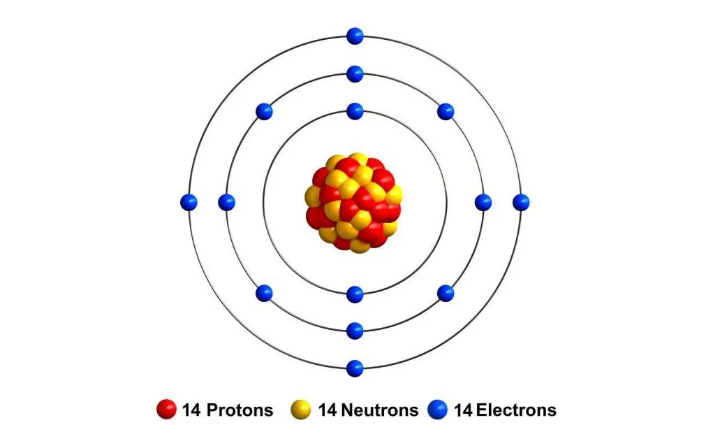
At the atomic scale, the 118 known elements include 92 occurring in nature; others are synthesized. The smallest representative unit of an element is the atom. An atom consists of a nucleus and orbiting electrons. The nucleus occupies only a tiny fraction of the atomic volume, so the effective size of an atom is determined by its electron cloud.
Electrons display wave-particle duality and do not follow definite orbits like macroscopic objects. Their positions are described probabilistically, forming an electron cloud around the nucleus.
Taking silicon, the most common semiconductor element, as an example: a silicon atom has 14 electrons, with 2 in the first shell, 8 in the second, and 4 valence electrons in the outermost shell. In crystalline silicon there are no obvious free electrons; the outer 4 electrons make silicon neither a conductor nor an insulator, giving it semiconductor properties. Silicon conducts electricity with a resistivity much higher than metals and its conductivity increases with temperature.
Atomic scale.
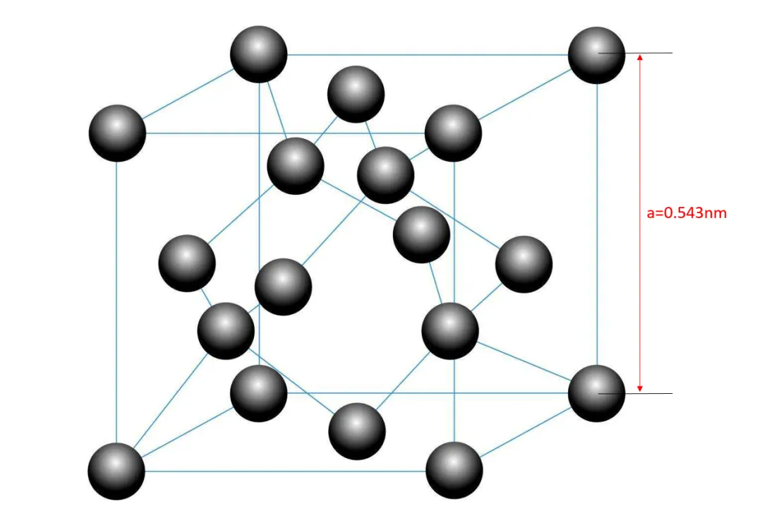
Atoms do not have a precisely defined outer boundary, so atomic radius is typically inferred from average interatomic distances. In crystalline silicon, the unit cell for the diamond cubic structure has lattice constant a = 0.543 nm at 300 K. The nearest-neighbor distance in the silicon plane shown is 0.384 nm, and three atoms side by side span 1.152 nm.
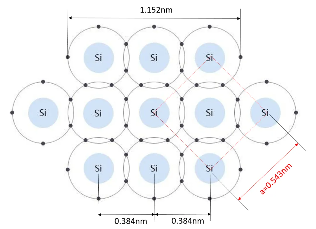
How many silicon atoms are in one cubic nanometer? A silicon face-centered cubic unit cell contains on average 8 atoms (8 × 1/8 + 6 × 1/2 + 4 = 8). With lattice constant a = 0.543 nm, 8 ÷ (0.5433) ≈ 50, so roughly 50 silicon atoms occupy 1 nm3. Doping silicon with a small amount of pentavalent or trivalent elements forms n-type or p-type semiconductors respectively but does not significantly change the lattice structure or atom count per volume. At the nanoscale atoms can be counted individually.
From atoms to function cells
We define a function cell as the smallest functional unit. In integrated circuits, a transistor can be considered a function cell. Resistors, capacitors, inductors, and diodes are also function cells. Function cells are composed of atoms and implement functions by controlling electrons. The realization of a function depends on practical needs and human ingenuity. The transistor is a typical function cell because it can control electron flow effectively.
The mainstream FinFET transistor allows current to flow from source to drain when a suitable voltage is applied to the gate, enabling switching behavior.
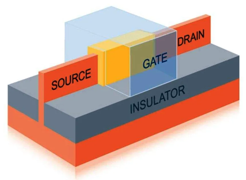
Using transistors to switch on and off represents different logic states. Multiple transistors combine to form logic circuits and implement higher-level functions.
Smaller function cells are generally preferable. What is the minimum scale of a function cell? Current silicon-based transistors face limits set by the smallest structural width and the transistor's area (volume).
Three silicon atoms side by side exceed 1 nm, so whether transistor feature sizes can reliably reach or go below 1 nm is still uncertain. Fabrication and theoretical operation at that scale are challenging.
Novel devices such as single-atom transistors have a minimum structural width equal to a single atom and control conduction by manipulating individual atoms. Reported energy consumption for single-atom transistors could be orders of magnitude lower than silicon transistors, which would be advantageous for future applications.
From function cells to common systems
Function cells can be very small: current technology supports integrating over ten billion transistors on a chip the size of a fingernail. Multiple function cells form function blocks, which form function units, which in turn form microsystems. For consumer products, system sizes must suit human use: for example, phones are sized for hand-held use and laptops for desktop or lap use.
We call systems intended for regular human interaction common systems. They consist of microsystems and function units, ultimately built from function cells. Because common systems must match human scale, their external dimensions change little even as internal function density increases. Over time, the number of function cells inside these systems rises, increasing system function density, which follows what may be called a Function Density Law.
From common systems to giant systems
Other systems serve groups or large-scale applications and can be very large; these are giant systems. Examples include crewed spacecraft systems, wireless communication networks, and global navigation satellite systems. Giant systems are typically complex and composed of many common systems, microsystems, or function units.
For example, a GPS system has three major parts: a space segment of 24 satellites, a ground segment with a master control station, monitoring stations, and ground antennas, and the user equipment segment consisting of various GPS receivers. GPS provides real-time high-precision positioning, velocity, and timing for vehicles, ships, aircraft, satellites, and spacecraft.
Like common systems, giant systems increase their function density over time to meet more demands, following the same function density trend.
Summary of integration scales
We divide electronic systems into six hierarchical levels: function cell, function block, function unit, microsystem, common system, and giant system.
We further analyze the function cell into four hierarchical levels: elementary particles form atoms, atoms form unit cells, and unit cells form function cells.
From elementary particles to the most complex systems achievable by humans, we describe nine hierarchical levels. The function cell is the critical link, the basic carrier of function, analogous to biological cells in living organisms. Each level requires exploration, implementation, innovation, and development by different specialists.
Integration
2 Dimensions of Integration
Humans perceive a three-dimensional space plus time, often called four-dimensional spacetime. Higher-dimensional theories exist in physics but are beyond practical perception and have little direct impact on most engineering activities.
In common terms, 0D is a point, 1D a line, 2D a plane, and 3D a volume. Integration involves bringing multiple units together to realize function, so practical integration uses mainly planar (2D) and volumetric (3D) approaches.
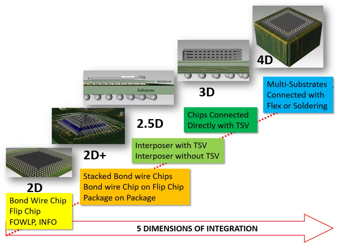
Practical classification using only 2D and 3D can be limiting. Terms such as "pseudo-3D" and "true 3D" are sometimes used for different chip stacking approaches. For clarity, this article defines five integration dimensions: 2D, 2D+, 2.5D, 3D, and 4D, and uses two important criteria: physical structure and electrical interconnect.
The following descriptions focus mainly on IC packaging, but the concepts apply more broadly.
2D integration
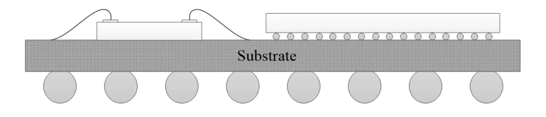
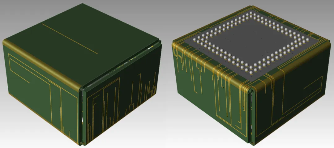
2D integration mounts all chips and passive components flat on the surface of a substrate.
Using the substrate top surface XY plane and the substrate normal as the Z axis, a coordinate system is established. Physical structure: all chips and passive components contact the substrate plane; substrate routing and vias are below the XY plane. Electrical interconnect: connections are made through the substrate except for rare bond points connected directly by wires.
Common 2D technologies include MCM, some SiP implementations, and PCBs.
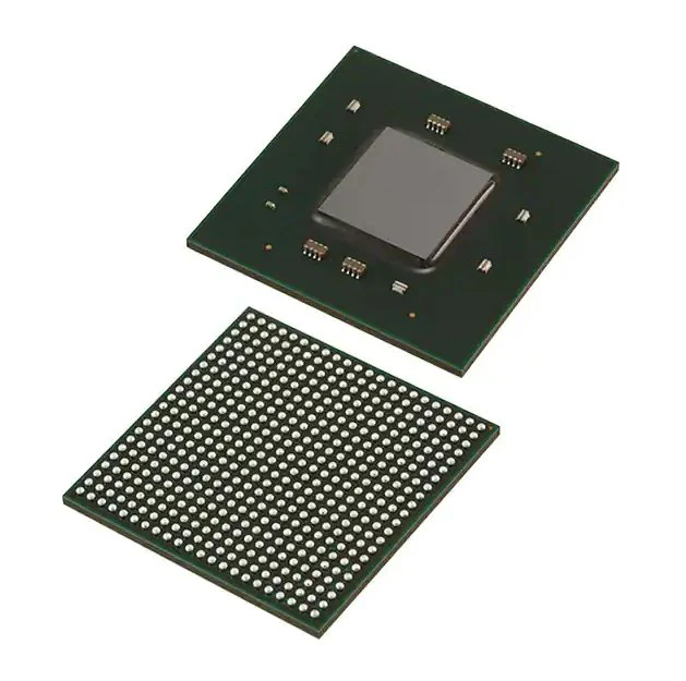
MCM (multi-chip module) densely mounts multiple bare chips on a common substrate to form a complete module.
In traditional packaging, packages served individual chips for protection and interconnection and did not embody the concept of integration. MCM introduced integration into packaging, shifting the packaging concept from a single chip to a module or system.
2D SiP follows a similar process to MCM but on a larger scale and can form standalone systems.
2D integration schematic
Wafer-level fan-out packaging such as FOWLP-based integrations, although lacking a traditional substrate, can be classified as 2D integration. Transistor layouts on silicon are also fundamentally 2D. 2D integration is simplest for EDA design tools.
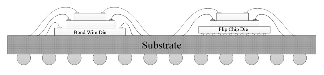
2D+ integration
2D+ describes traditional stacked-chip integration using bond wires. Although the physical arrangement is three-dimensional, it is classified as 2D+ for two reasons: 1) current usage of "3D integration" often specifically denotes TSV-based integration, so this distinction avoids confusion; 2) electrically these stacks still rely on the substrate for interconnect, like 2D integration, but save package area through vertical stacking.
Physical structure: chips and passives are located above the XY plane; some chips do not touch the substrate directly while substrate routing and vias remain below the XY plane. Electrical interconnect: connections still go through the substrate except for rare bond points.
The following examples are 2D+ integrations.
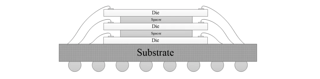
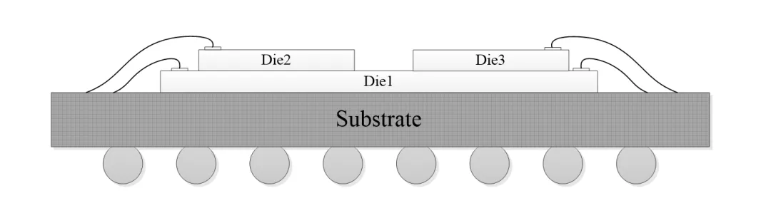
2D+ integration schematic
Package-on-package (PoP) approaches can be classified as 2D+ based on their physical and electrical connections. EDA tools have long supported 2D+ design.
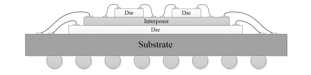
2.5D integration
2.5D sits between 2D and 3D. It combines 2D characteristics with some 3D aspects; strictly speaking 2.5D is a classification convenience rather than a physical dimension.
Physical structure: chips and passives are above the XY plane, with at least some mounted on an interposer. Routing and vias exist on the interposer above the XY plane and on the substrate below it. Electrical interconnect: the interposer provides electrical connections for chips mounted on it.
The interposer is the key. Variations include silicon interposers with TSVs, silicon interposers without TSVs, glass interposers with TGVs, or other materials. Silicon interposers with TSVs are common: chips connect to the interposer via microbumps, the interposer connects to the substrate via bumps, and the silicon interposer uses RDL routing and TSVs for through-layer connections. This 2.5D approach is suitable for large chips with high pin density and typically uses flip-chip mounting.
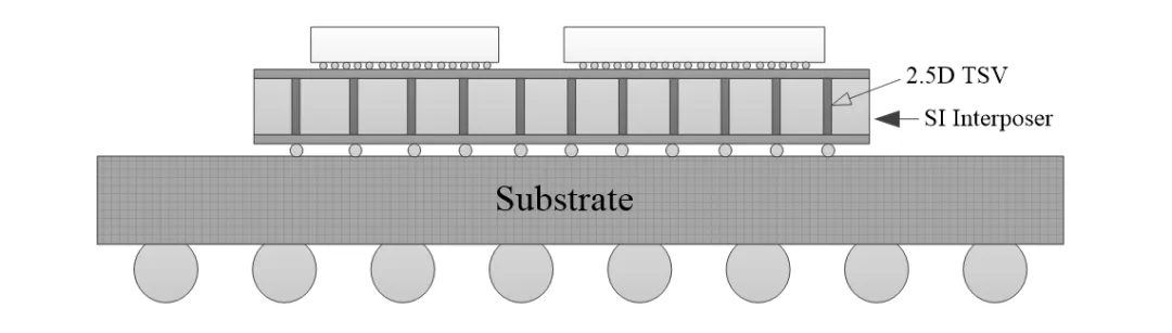
2.5D with TSVs schematic
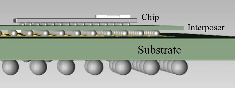
2.5D without TSVs typically has a large bare chip mounted on the substrate (connected by bond wires or flip chip) with smaller chips mounted above on an interposer. The interposer routes signals to its edges and connects to the substrate by bond wires. Such interposers often do not require TSVs and rely on top-layer RDLs for interconnect.
2.5D without TSVs schematic
EDA tools now support 2.5D designs well.
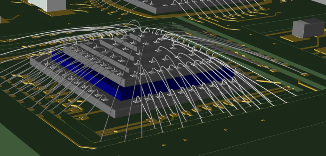
3D integration
The main difference between 2.5D and 3D is that 2.5D routes and vias are implemented on an interposer, while 3D implements vias (TSVs) and routing directly through and on the chips, enabling direct electrical connections between stacked chip layers.
Physical structure: chips and passives are above the XY plane, chips are stacked vertically, TSVs traverse the stacked chips, and substrate routing and vias exist below the XY plane. Electrical interconnect: chips are directly connected via TSVs and RDLs.
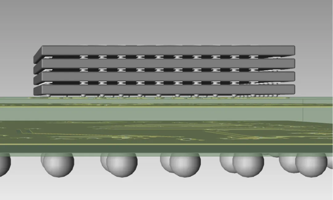
3D integration is commonly used for stacking homogeneous chips, such as memory stacks (DRAM stack, NAND flash stack), where identical chips are vertically stacked and interconnected via TSVs.
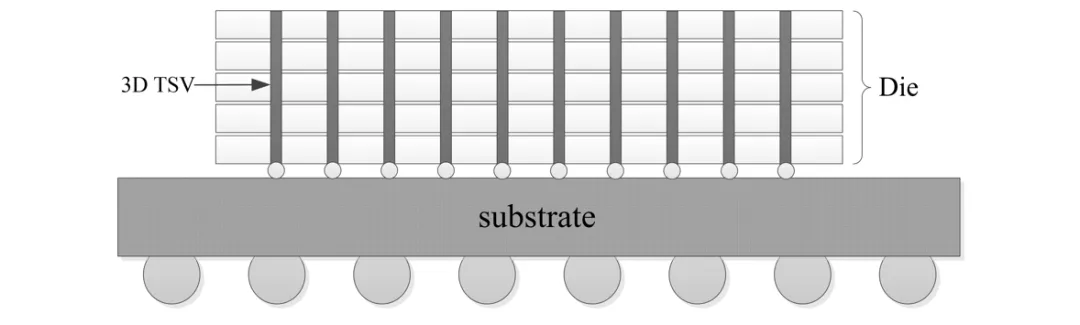
Schematic of homogeneous-chip 3D integration. For heterogeneous 3D integration, different chip types are stacked and connected via TSVs and may use surface RDLs to connect TSVs between layers.
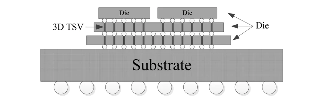
Schematic of heterogeneous-chip 3D integration
Manufacturing 3D NAND Flash by creating multiple storage layers directly on the chip is also a form of 3D integration. EDA tools now provide good support for 3D designs.
4D integration
So far we have described 2D, 2D+, 2.5D, and 3D. How is 4D defined?
In the previously described integration types, each substrate, interposer, and chip has a Z axis that is vertically aligned so that all substrates and chips are parallel. In 4D integration this is not the case.
When the XY planes of multiple substrates are not parallel, i.e., the Z axes of different substrates are tilted relative to each other, we call this 4D integration. Physical structure: multiple substrates are mounted in nonparallel orientations, each populated with components using diverse mounting methods. Electrical interconnect: substrates are connected by flex circuits, solder, or other means, and on-substrate chip interconnections are diversified.
4D integration using rigid-flex substrates schematic
Hermetic ceramic 4D integration schematic
4D integration is defined by the orientations and interconnections of multiple substrates. Each substrate in a 4D assembly may itself contain 2D, 2D+, 2.5D, or 3D integration. 4D techniques address issues that parallel 3D stacks cannot, offering more flexible placement, better thermal solutions for high-power chips, and hermetic packaging options needed for aerospace applications. EDA tools are increasingly supporting 4D design.
4D design example in EDA tools
4D integration increases flexibility and diversity in integration strategies. From a strict physical standpoint, objects are three-dimensional, but classifying integration as 2D, 2D+, 2.5D, 3D, and 4D is useful for differentiating approaches.
Summary of integration dimensions
The following figure summarizes the five integration dimensions and provides EDA examples and the types included in each dimension.
Postscript
Integration is a human activity and a key method for transforming the world. This article has analyzed modern electronic integration in terms of spatial scale and spatial dimension. Scale ranges from elementary particles to the most complex systems and is divided into nine levels; dimension is categorized into five types for classification. The two directions in integrated circuit development are smaller scales and higher dimensions, which complement each other and together drive technological progress.