 ALLPCB


If you're looking to enhance your PCB design with better signal integrity and reduced electromagnetic interference (EMI), mastering the inner layer stackup, particularly the placement of power and ground planes, is crucial. In this comprehensive guide, we'll dive into the essentials of PCB inner layer power plane design, ground plane placement inner layer, and stackup optimization inner layer to help you create efficient and reliable printed circuit boards. Whether you're a beginner or an experienced engineer, this blog offers actionable insights to improve your designs.
Why Inner Layer Stackup Matters in PCB Design
The stackup of a printed circuit board (PCB) refers to the arrangement of its layers, including signal layers, power planes, and ground planes. A well-designed stackup ensures proper signal routing, minimizes noise, and maintains power integrity. Inner layers, in particular, play a vital role because they often house critical power and ground planes that directly impact the board's performance.
A poorly optimized stackup can lead to issues like crosstalk, EMI, and signal delays. For instance, improper placement of power and ground planes can result in impedance mismatches, causing signal reflections that degrade performance. By focusing on stackup optimization inner layer, you can avoid these pitfalls and achieve a more stable and efficient design.
Key Principles of PCB Inner Layer Stackup Design
Designing an effective inner layer stackup requires careful planning. Let's explore the fundamental principles that guide this process, focusing on layer arrangement and the roles of power and ground planes.
1. Understanding Layer Count and Arrangement
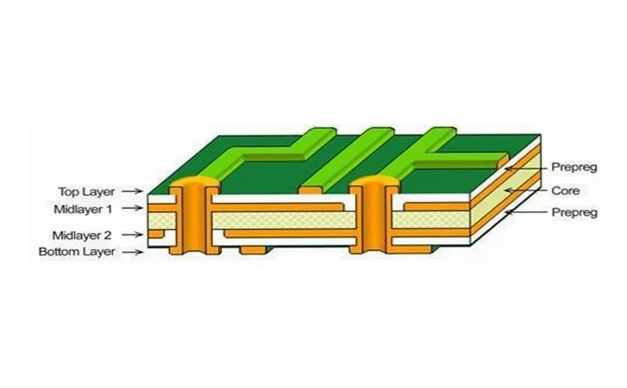
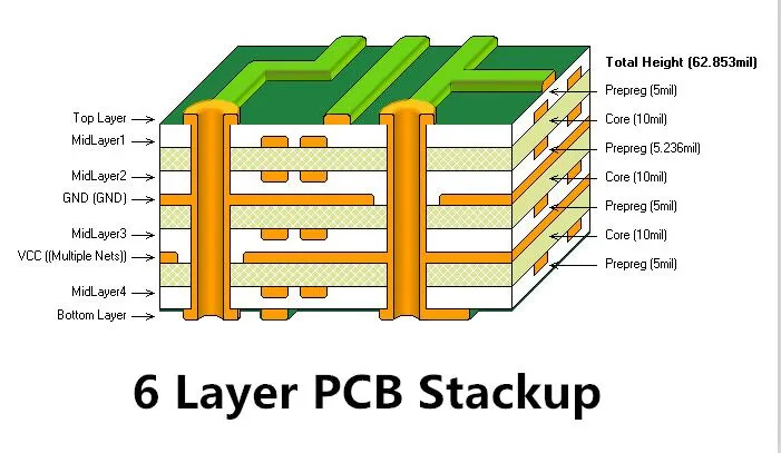
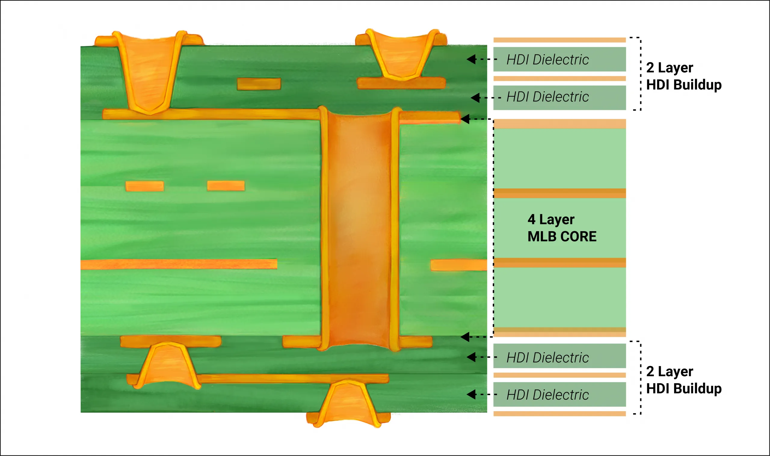
The number of layers in a PCB depends on the complexity of the design. A 4-layer board is common for simpler projects, while 6, 8, or even 10-layer boards are used for high-speed or high-density designs. Inner layers typically consist of power and ground planes, which provide stable voltage distribution and a low-impedance return path for signals.
For a 4-layer PCB, a common stackup might look like this:
- Top Layer: Signal routing
- Inner Layer 1: Ground plane
- Inner Layer 2: Power plane
- Bottom Layer: Signal routing
In a 6-layer board, you might add more signal layers while maintaining dedicated power and ground planes in the inner layers. The goal of stackup optimization inner layer is to keep power and ground planes close to each other to reduce loop inductance and improve decoupling.
2. Balancing Signal Integrity and Power Distribution
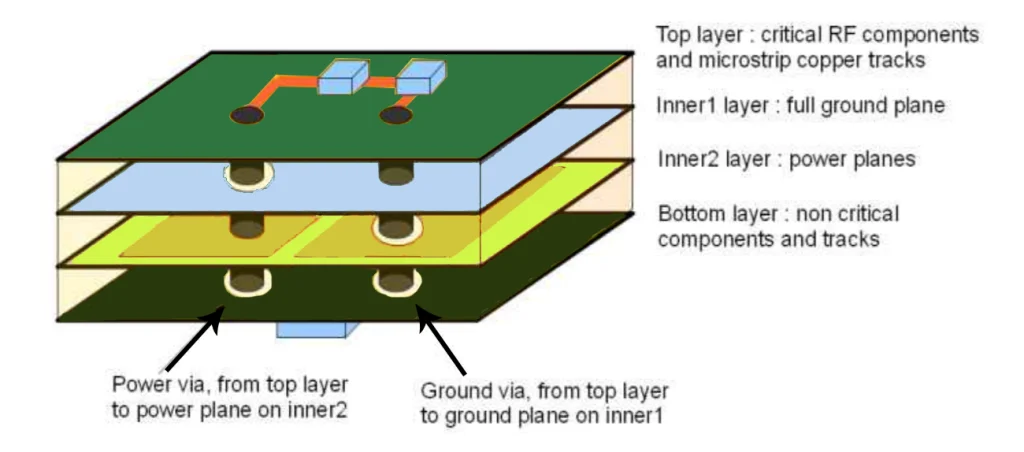
Signal integrity is a top priority in PCB design. High-speed signals, such as those running at 1 GHz or higher, are prone to interference if not properly managed. Placing a ground plane adjacent to signal layers provides a consistent return path, reducing noise. Similarly, a power plane ensures a stable voltage supply to components, minimizing voltage drops.
For example, in high-speed designs, a signal layer should ideally be next to a ground plane to maintain controlled impedance, often targeting a value like 50 ohms for single-ended traces. This proximity reduces the loop area for return currents, cutting down on EMI.
Optimizing Power Plane Design in Inner Layers
The power plane in a PCB's inner layer is responsible for delivering a stable voltage to all components. Poor PCB inner layer power plane design can lead to voltage drops, noise, and inefficient power distribution. Here are some strategies to optimize power planes:
1. Use Dedicated Power Planes for Different Voltages
In designs with multiple voltage levels (e.g., 3.3V and 5V), avoid splitting a single power plane into sections. Instead, dedicate separate inner layers to each voltage. This approach prevents interference between different power domains and ensures cleaner power delivery.
2. Minimize Power Plane Interruptions
Cuts or splits in a power plane can disrupt current flow, leading to voltage drops. Keep the plane as continuous as possible. If splits are unavoidable due to design constraints, place decoupling capacitors near the split to maintain voltage stability. A typical decoupling capacitor value for high-frequency noise suppression might be 0.1 μF.
3. Place Power Planes Close to Ground Planes
Positioning power and ground planes adjacent to each other creates a natural capacitance between them, which helps filter out high-frequency noise. For instance, in a 4-layer board, placing the ground plane on layer 2 and the power plane on layer 3 minimizes the distance between them, enhancing this effect.
Best Practices for Ground Plane Placement in Inner Layers
The ground plane serves as a reference point for signals and a shield against EMI. Proper ground plane placement inner layer is essential for maintaining signal integrity and reducing noise. Here are key tips to follow:
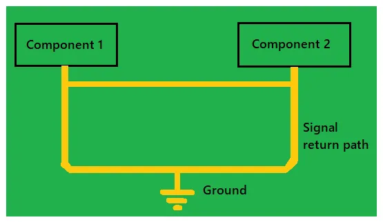
1. Dedicate an Entire Layer to Ground
In multi-layer PCBs, at least one inner layer should be a solid ground plane without interruptions. This continuous plane provides a low-impedance path for return currents, reducing the risk of ground bounce—a phenomenon where the ground voltage fluctuates due to high-speed switching.
2. Position Ground Planes Near Signal Layers
High-speed signal layers should be adjacent to a ground plane to maintain a consistent return path. For example, in a 6-layer stackup, if layers 1 and 6 are signal layers, layers 2 and 5 should ideally be ground planes. This arrangement helps control impedance and reduces crosstalk between traces.
3. Avoid Splitting Ground Planes
Splitting a ground plane can create separate ground regions, forcing return currents to take longer paths and increasing noise. If a split is necessary, ensure that return paths are not disrupted by placing vias or stitching capacitors to connect the split regions.
Advanced Techniques for Stackup Optimization in Inner Layers
Beyond basic layer arrangement, stackup optimization inner layer involves advanced techniques to address specific challenges in high-speed and high-density designs. Let's explore some of these methods.
1. Impedance Control Through Dielectric Thickness
The dielectric material between layers affects the impedance of signal traces. For high-speed signals, maintaining a specific impedance (e.g., 50 ohms for single-ended or 100 ohms for differential pairs) is critical. Adjust the thickness of the dielectric between a signal layer and its adjacent ground plane to achieve the desired impedance. For instance, a thinner dielectric (e.g., 5 mils) can lower impedance, while a thicker one (e.g., 10 mils) increases it.
2. Via Design for Inner Layer Connections
Vias connect traces between layers, but they can introduce signal reflections if not designed properly. Use microvias or buried vias for inner layer connections to minimize stub effects, especially in high-speed designs. Additionally, place ground vias near signal vias to provide a return path and reduce noise.
3. Thermal Management in Power Planes
Power planes can generate heat, especially in high-current applications. To manage this, ensure adequate copper thickness (e.g., 1 oz or 2 oz per square foot) on power planes to handle current without overheating. You can also add thermal vias to dissipate heat to outer layers or heat sinks.
Common Mistakes to Avoid in Inner Layer Stackup Design
Even experienced engineers can make mistakes when designing inner layer stackups. Here are some pitfalls to watch out for:
- Neglecting Ground Plane Continuity: Breaks in the ground plane can disrupt return paths, leading to EMI and signal issues. Always prioritize a solid ground plane.
- Improper Power Plane Splits: Splitting power planes without proper decoupling can cause voltage instability. Use capacitors strategically near splits.
- Ignoring Layer Symmetry: An unbalanced stackup can cause warping during manufacturing. Ensure symmetry in layer arrangement and dielectric thickness.
Tools and Resources for Stackup Design
Designing an optimized inner layer stackup requires the right tools. Many PCB design software platforms offer stackup editors that allow you to define layer arrangements, materials, and thicknesses. These tools often include impedance calculators to help you achieve the desired values for signal traces.
Additionally, consult with your PCB manufacturer early in the design process. They can provide guidance on material choices, layer counts, and manufacturing constraints to ensure your stackup is feasible and cost-effective.
Conclusion: Building Better PCBs with Optimized Inner Layers
Mastering PCB inner layer power plane design, ground plane placement inner layer, and stackup optimization inner layer is a game-changer for creating high-performance printed circuit boards. By carefully arranging power and ground planes, maintaining signal integrity, and using advanced techniques like impedance control and via design, you can significantly improve your PCB's reliability and efficiency.
Start by planning your stackup based on the specific needs of your project, whether it's a simple 4-layer board or a complex 10-layer design. Pay attention to the placement of power and ground planes, avoid common mistakes, and leverage design tools to refine your approach. With these strategies, you'll be well on your way to designing PCBs that meet the highest standards of performance.


