 ALLPCB


In the world of high-speed PCB design, signal quality is everything. One critical technique to enhance signal integrity is backdrilling blind vias to reduce stub length. But how do you backdrill blind vias effectively, and why does stub length reduction matter? This blog post will guide you through the process, explaining the importance of backdrilling for signal quality and offering practical steps to implement it in your designs. Whether you're an engineer working on high-speed circuits or a designer looking to optimize performance, you'll find actionable insights here.
At its core, backdrilling is a manufacturing process that removes unused portions of a via, known as stubs, to minimize signal reflections and interference. By focusing on blind vias—vias that connect specific layers without passing through the entire board—you can achieve even greater control over signal quality. Let’s dive into the details of backdrilling, stub length reduction, and their impact on high-speed PCB design.
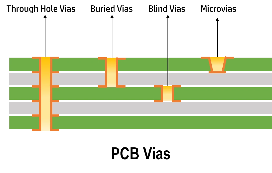
What Are Blind Vias and Why Do They Matter in PCB Design?
Blind vias are a type of vertical interconnect in a printed circuit board (PCB) that connect an outer layer to one or more inner layers without going through the entire board. Unlike through-hole vias, which span the full thickness of the PCB, blind vias are drilled only to a specific depth. This makes them ideal for high-density designs where space is limited, and layer-to-layer connections must be precise.
In high-speed PCB design, blind vias play a crucial role. They help reduce the overall via length, which can minimize signal delays and impedance mismatches. However, even with blind vias, a small unused portion, or stub, can remain at the end of the via. This stub can act like an antenna, causing signal reflections and degrading performance, especially at frequencies above 5 GHz. This is where backdrilling comes into play as a solution for stub length reduction.
Understanding Via Stubs and Their Impact on Signal Quality
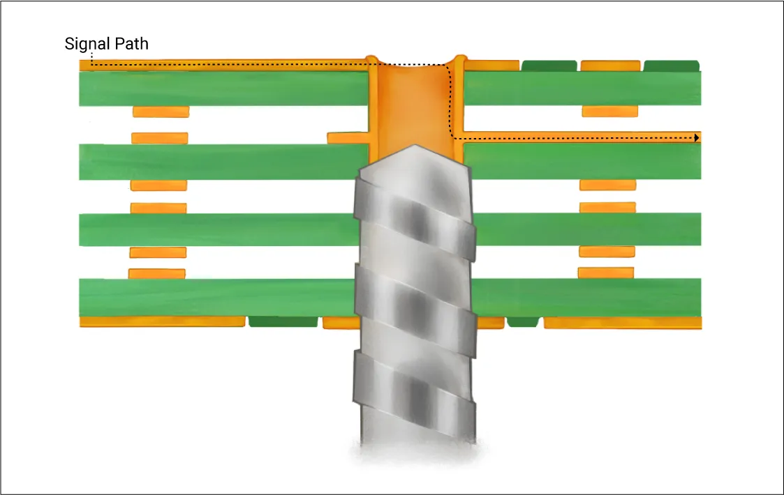
A via stub is the unused portion of a via that extends beyond the point where a signal is routed to another layer. In high-speed designs, these stubs can cause significant issues. When a signal travels through a via, the stub can create a resonance effect, leading to reflections that interfere with the original signal. This results in signal degradation, increased noise, and potential data errors.
For example, in a design operating at 10 Gbps, a via stub as short as 0.5 mm can introduce enough reflection to cause a noticeable drop in signal quality. The longer the stub, the worse the effect, especially at higher frequencies. Stub length reduction is, therefore, a critical step in maintaining signal integrity for applications like telecommunications, data centers, and high-performance computing.
Backdrilling blind vias offers a way to physically remove these stubs, ensuring that the signal path is as clean as possible. By eliminating the unused portion of the via, you can reduce reflections and improve overall performance.
What Is Backdrilling and How Does It Work?
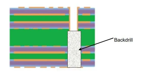
Backdrilling, also known as controlled-depth drilling, is a manufacturing technique used to remove the unused stub of a via after it has been plated. The process involves drilling into the via from the opposite side of the board to a precise depth, ensuring that only the stub is removed without damaging the functional part of the via.
In the case of blind vias, backdrilling is slightly more complex because the via does not extend through the entire board. However, the principle remains the same: identify the unused portion of the via and carefully remove it. This process is typically done using advanced CNC drilling machines with precise depth control to avoid over-drilling or damaging nearby traces.
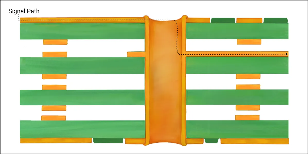
The result of backdrilling blind vias is a shorter effective via length, which directly translates to stub length reduction. This, in turn, minimizes signal reflections and improves signal quality, making backdrilling a must-have technique for high-speed PCB design.
Why Focus on Stub Length Reduction in High-Speed Designs?
In high-speed PCB design, every millimeter of a signal path matters. As data rates climb beyond 10 Gbps and into the realm of 25 Gbps or higher, even tiny imperfections like via stubs can cause significant signal loss. Stub length reduction through backdrilling offers several key benefits:
- Reduced Signal Reflections: Stubs cause reflections that interfere with the main signal. Removing them ensures a cleaner signal path.
- Lower Crosstalk: Shorter vias reduce the chance of electromagnetic interference between adjacent signals.
- Improved Impedance Matching: Stubs can create impedance discontinuities. Backdrilling helps maintain a consistent impedance, often around 50 ohms for high-speed signals.
- Better Eye Diagrams: In signal integrity testing, backdrilled vias result in wider, clearer eye diagrams, indicating better data transmission quality.
For instance, in a design operating at 28 Gbps, a stub length of just 0.3 mm can degrade the signal-to-noise ratio by over 10%. Backdrilling can eliminate this issue, ensuring reliable performance even at extreme speeds.
Step-by-Step Guide to Backdrilling Blind Vias
Now that we understand the importance of backdrilling and stub length reduction, let’s walk through the practical steps to implement this technique in your PCB design process. While the actual drilling is a manufacturing step, designers play a key role in preparing the board for success.
Step 1: Identify Critical Vias in Your Design
Start by analyzing your PCB layout to identify which blind vias carry high-speed signals. Focus on connections operating at frequencies above 5 GHz or data rates above 10 Gbps, as these are most susceptible to stub-related issues. Use simulation tools to model signal paths and pinpoint vias with significant stub lengths.
Step 2: Minimize Stub Length in the Design Phase
Before manufacturing, try to route signals in a way that minimizes stub length naturally. For blind vias, this might mean placing the via closer to the target layer or using sequential lamination to control via depth. While this won’t eliminate the need for backdrilling, it can reduce the amount of stub that needs to be removed.
Step 3: Specify Backdrilling Requirements
When preparing your design files, clearly indicate which blind vias require backdrilling. Provide detailed notes on the depth and diameter of the backdrill, ensuring that the manufacturer understands your intent. Typically, the backdrill diameter is slightly larger than the original via drill size (e.g., 0.1 mm larger) to ensure complete stub removal.
Step 4: Collaborate with Your Manufacturer
Work closely with your PCB manufacturer to confirm that they have the capability to perform precise backdrilling on blind vias. Share stack-up details and impedance requirements to ensure accuracy. Modern manufacturing equipment can achieve depth tolerances as tight as ±0.05 mm, which is critical for avoiding damage to functional via sections.
Step 5: Verify Results Post-Manufacturing
After fabrication, test the board for signal integrity using tools like a time-domain reflectometer (TDR) or vector network analyzer (VNA). Look for impedance discontinuities or reflections that might indicate incomplete stub removal. If issues persist, adjust the backdrilling parameters for future builds.
Best Practices for Backdrilling Blind Vias in High-Speed PCB Design
To get the most out of backdrilling and ensure optimal signal quality, follow these best practices:
- Use Simulation Tools: Before manufacturing, simulate your design to predict the impact of via stubs on signal quality. Tools like HyperLynx or Ansys can help you identify problem areas.
- Optimize Via Placement: Place blind vias strategically to minimize stub length even before backdrilling. Avoid routing high-speed signals through vias with long stubs if possible.
- Specify Tight Tolerances: Work with your manufacturer to ensure precise backdrilling depth control. Over-drilling can damage the via, while under-drilling leaves residual stubs.
- Test and Iterate: Signal integrity testing is key to validating your design. Use real-world data to refine your approach for future projects.
- Consider Alternatives: In some cases, technologies like buried vias or microvias might complement or replace backdrilling. Evaluate all options based on cost and performance needs.
Challenges and Limitations of Backdrilling Blind Vias
While backdrilling is a powerful technique for stub length reduction, it’s not without challenges. Understanding these limitations can help you plan your design more effectively.
- Manufacturing Complexity: Backdrilling blind vias requires advanced equipment and skilled operators, which can increase production costs by 10-20% compared to standard via processes.
- Design Constraints: Not all PCB layouts are suitable for backdrilling. Dense designs with closely spaced vias may risk damage during the process.
- Testing Needs: Post-manufacturing testing is essential to confirm that stubs have been removed without affecting via functionality. This adds time to the production cycle.
Despite these challenges, the benefits of improved signal quality often outweigh the drawbacks, especially for high-speed applications.
Real-World Applications of Backdrilling for Signal Quality
Backdrilling blind vias has become a standard practice in industries where high-speed signal integrity is non-negotiable. Here are a few examples:
- Telecommunications: In 5G infrastructure, backdrilling ensures that signals at 28 GHz and beyond maintain clarity over long distances.
- Data Centers: Servers handling 100 Gbps data rates rely on stub length reduction to minimize latency and errors.
- Aerospace: High-speed avionics systems use backdrilled vias to ensure reliable communication under extreme conditions.
By applying backdrilling techniques, designers in these fields can push the boundaries of performance while maintaining signal quality.
Conclusion: Elevate Your High-Speed PCB Design with Backdrilling
Backdrilling blind vias is a game-changer for high-speed PCB design. By focusing on stub length reduction, you can significantly improve signal quality, reduce reflections, and ensure reliable performance even at the highest data rates. From identifying critical vias to collaborating with manufacturers, the steps outlined in this guide provide a clear path to success.
As signal speeds continue to increase, mastering techniques like backdrilling becomes essential for staying ahead in the industry. Whether you're designing for telecommunications, data centers, or other high-performance applications, prioritizing signal integrity through stub length reduction will set your projects apart.
With the right tools, planning, and manufacturing support, backdrilling blind vias can become a seamless part of your design workflow. Take the time to implement these practices, and watch as your PCB designs achieve new levels of performance and reliability.


