 ALLPCB


In the world of high-speed electronics, achieving impedance matching in multilayer PCBs is crucial for ensuring signal integrity and minimizing data loss. For engineers working with high-speed signals, improper impedance can lead to reflections, crosstalk, and degraded performance. So, how do you achieve impedance matching in multilayer PCBs? The key lies in understanding transmission line structures like microstrip and stripline, carefully designing trace geometries, selecting appropriate materials, and using simulation tools to validate your design.
In this comprehensive guide, we'll walk you through the essentials of impedance matching for multilayer PCBs, focusing on high-speed signals. We'll cover the importance of controlled impedance, the differences between microstrip impedance and stripline impedance, and provide actionable steps to ensure your PCB design meets the demands of modern electronics. Whether you're designing for telecommunications, computing, or other high-speed applications, this blog will equip you with the knowledge to optimize your multilayer PCB designs.
What Is Impedance Matching and Why Does It Matter for High-Speed Signals?
Impedance matching refers to the process of designing a circuit so that the impedance of the source, transmission line, and load are equal. In the context of multilayer PCBs handling high-speed signals, this means ensuring that the traces carrying signals have a consistent impedance—often 50 ohms or 100 ohms for differential pairs—to prevent signal reflections. Reflections occur when there's a mismatch, causing part of the signal to bounce back, which can distort data and increase noise.
For high-speed signals, such as those operating at frequencies above 100 MHz, even small mismatches can lead to significant issues. These signals are common in applications like USB, HDMI, PCIe, and DDR memory interfaces. Without proper impedance matching, you risk signal degradation, timing errors, and electromagnetic interference (EMI). In multilayer PCBs, where traces are routed across multiple layers with varying dielectric properties, achieving controlled impedance becomes even more complex but essential.
Understanding Multilayer PCBs and High-Speed Signal Challenges
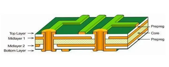
Multilayer PCBs consist of multiple layers of conductive traces separated by insulating materials (dielectrics). These boards are used in complex designs to save space and route numerous signals efficiently. However, the layered structure introduces challenges for high-speed signals, including:
- Signal Coupling: Traces on adjacent layers can interfere with each other, causing crosstalk.
- Dielectric Variations: Different materials and layer thicknesses can affect signal speed and impedance.
- Routing Complexity: High-speed signals often require specific routing paths to avoid interference and maintain impedance.
To tackle these challenges, designers must focus on impedance matching by controlling trace width, spacing, and the dielectric environment around the traces. This is where transmission line structures like microstrip and stripline come into play.
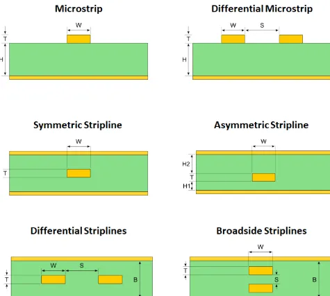
Microstrip vs. Stripline: Key Differences in Impedance Control
In multilayer PCBs, two primary transmission line structures are used for routing high-speed signals: microstrip and stripline. Each has unique characteristics that affect impedance matching.
What Is Microstrip Impedance?
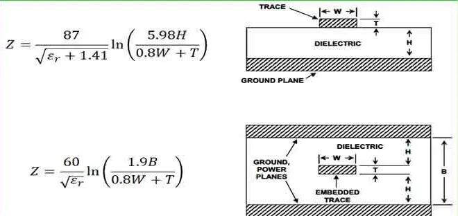
Microstrip traces are routed on the outer layers of a PCB, with a ground plane directly beneath them. The impedance of a microstrip line depends on the trace width, the distance to the ground plane, and the dielectric constant of the material between them. Typically, microstrip lines are easier to fabricate and test since they are on the surface, but they are more susceptible to EMI due to their exposed nature.
For a standard 50-ohm microstrip line on a common FR-4 material (dielectric constant of about 4.2), the trace width might be around 6-8 mils for a 10-mil thick dielectric layer. However, these values can vary based on the specific PCB stack-up and materials used.
What Is Stripline Impedance?
Stripline traces, on the other hand, are embedded between two ground planes within the PCB. This structure offers better shielding from EMI and crosstalk, making it ideal for high-speed signals in dense multilayer designs. Stripline impedance is influenced by trace width, the distance between the ground planes, and the dielectric constant of the surrounding material.
For a 50-ohm stripline in a similar FR-4 material, the trace width might be slightly narrower (around 5-7 mils) due to the dual ground planes providing a more controlled environment. Stripline designs often require more precise manufacturing, as any misalignment in layer registration can affect impedance.
Steps to Achieve Impedance Matching in Multilayer PCBs
Now that we understand the basics of microstrip and stripline impedance, let’s dive into the practical steps to achieve impedance matching for high-speed signals in multilayer PCBs. Follow these guidelines to ensure signal integrity in your designs.
1. Define Impedance Requirements Early
Start by identifying the impedance requirements for your high-speed signals. Common standards include 50 ohms for single-ended signals and 100 ohms for differential pairs. Check the specifications of the components and interfaces you're working with (e.g., USB 3.0 typically requires 90 ohms differential impedance). Defining these values upfront helps guide your PCB stack-up and trace design.
2. Design the PCB Stack-Up for Controlled Impedance
The stack-up of your multilayer PCB plays a critical role in impedance matching. Decide where to place signal layers, ground planes, and power planes. For high-speed signals:
- Place ground planes adjacent to signal layers to provide a consistent reference for impedance calculations.
- Use symmetrical stack-ups for stripline designs to ensure uniform dielectric thickness around traces.
- Minimize the distance between signal traces and their reference planes to reduce impedance variations.
For example, in a 6-layer PCB, you might allocate layers 1 and 6 for microstrip signals, layers 3 and 4 for stripline signals, and layers 2 and 5 as ground planes. Work with your PCB manufacturer to finalize the stack-up, as they can provide precise dielectric constants and layer thicknesses.
3. Calculate Trace Widths and Spacing
Use impedance calculators or simulation software to determine the appropriate trace width and spacing for your target impedance. These tools account for factors like dielectric constant (typically 4.2 for FR-4), trace thickness (often 1 oz copper, or 1.4 mils), and layer spacing. For differential pairs, ensure consistent spacing between the traces to maintain the required differential impedance.
As a rule of thumb, wider traces lower impedance, while narrower traces increase it. For a 50-ohm microstrip on FR-4 with a 10-mil dielectric height, a trace width of around 7 mils is often a good starting point. Adjust based on your specific stack-up.
4. Select the Right Materials
The dielectric material in your PCB affects signal propagation and impedance. FR-4 is common for many designs, but for very high-speed signals (above 5 GHz), consider low-loss materials like Rogers or Isola, which have more stable dielectric constants (often around 3.0 to 3.5) and lower loss tangents. These materials reduce signal attenuation and help maintain consistent impedance across frequencies.
5. Route High-Speed Signals Carefully
When routing high-speed signals, follow best practices to avoid impedance discontinuities:
- Keep trace lengths as short as possible to minimize signal delay and loss.
- Avoid sharp bends; use 45-degree angles or curved traces to prevent reflections.
- Maintain consistent trace width and spacing, especially for differential pairs.
- Route critical signals away from noisy areas like power lines or switching components.
For multilayer PCBs, consider using vias sparingly, as they can introduce impedance mismatches. If vias are necessary, use back-drilling to remove unused via stubs that can cause reflections.
6. Simulate and Validate Your Design
Before sending your design for fabrication, use simulation tools to verify impedance matching. Software like field solvers can model the electromagnetic behavior of your traces and predict impedance values. Compare simulated results with your target impedance, and tweak trace widths or stack-up if needed. Post-fabrication, you can use a time-domain reflectometer (TDR) to measure actual impedance and ensure it matches your design goals.
Common Pitfalls to Avoid in Impedance Matching
Even with careful planning, mistakes can happen. Here are some common pitfalls to watch out for when designing multilayer PCBs for high-speed signals:
- Ignoring Manufacturing Tolerances: Trace widths and dielectric thicknesses can vary slightly during fabrication. Account for these tolerances (often ±10%) in your design by consulting with your manufacturer.
- Inconsistent Reference Planes: Ensure that ground or power planes used as reference layers are continuous under high-speed traces. Breaks or splits can cause impedance mismatches.
- Overlooking Via Effects: Vias can introduce inductance and capacitance, disrupting impedance. Minimize their use or optimize via design for high-speed paths.
- Neglecting Frequency Dependence: At very high frequencies, skin effect and dielectric losses can alter impedance. Use materials suited for your operating frequency range.
Advanced Tips for Optimizing Impedance in High-Speed Designs
For engineers tackling particularly challenging designs, consider these advanced strategies:
- Differential Pair Matching: For differential signals, ensure both traces are of equal length and maintain consistent spacing to avoid skew and impedance mismatch.
- Embedded Capacitance: Use thin dielectric layers between power and ground planes to create embedded capacitance, reducing noise and stabilizing impedance for high-speed signals.
- Hybrid Designs: Combine microstrip and stripline routing in the same PCB to balance cost and performance. Use microstrip for less critical signals on outer layers and stripline for sensitive high-speed signals internally.
Conclusion: Mastering Impedance Matching for Multilayer PCBs
Achieving impedance matching in multilayer PCBs for high-speed signals is a critical skill for modern electronics design. By understanding the differences between microstrip impedance and stripline impedance, designing a proper stack-up, calculating trace geometries, and validating your work through simulation, you can ensure signal integrity and minimize issues like reflections and EMI. Remember to select the right materials, follow routing best practices, and account for manufacturing tolerances to create reliable, high-performance PCBs.
With the steps and tips outlined in this guide, you're well-equipped to tackle the challenges of impedance matching in your next multilayer PCB project. Focus on precision and collaboration with your manufacturing partner to bring your high-speed designs to life with confidence.


