 ALLPCB


If you're working on a mixed-signal PCB and struggling with noise and interference between analog and digital circuits, proper through-hole via design and placement can make a significant difference. In this blog, we’ll explore how strategic via placement and design techniques can minimize noise and interference in mixed-signal PCBs, ensuring optimal performance for both analog and digital components. We’ll dive deep into practical tips, specific guidelines, and technical details to help you achieve a cleaner, more reliable design.
What Are Mixed-Signal PCBs and Why Is Noise a Challenge?
Mixed-signal PCBs are circuit boards that combine analog and digital circuits on the same substrate. Analog circuits handle continuous signals, such as audio or sensor data, while digital circuits process discrete signals, like binary data in microcontrollers. The coexistence of these two types of signals often leads to noise and interference issues. Digital circuits, with their fast-switching signals, generate electromagnetic interference (EMI) that can disrupt the sensitive analog components. Meanwhile, analog signals can introduce unwanted noise into digital systems if not properly managed.
Noise in mixed-signal designs can degrade signal integrity, cause data errors, or even lead to complete system failure. This is where through-hole vias come into play. Vias are conductive pathways that connect different layers of a PCB, and their design and placement directly impact how noise and interference travel through the board. Poorly placed vias can act as antennas, picking up or radiating EMI, while well-designed vias can help isolate noisy signals and maintain clean power distribution.
In the sections below, we’ll break down the role of through-hole vias in noise reduction and provide actionable strategies for optimizing their design in mixed-signal PCBs.
The Role of Through-Hole Vias in Mixed-Signal PCB Design
Through-hole vias are vertical connections drilled through a PCB to link traces on different layers. Unlike surface-mount vias, they pass completely through the board, providing robust connections for power, ground, and signal paths. In mixed-signal designs, vias are critical for maintaining signal integrity and reducing interference between analog and digital circuits.
Here’s why through-hole vias matter for noise reduction:
- Grounding and Shielding: Vias connect ground planes across layers, creating a low-impedance path for return currents. This helps contain EMI and prevents it from coupling into sensitive analog circuits.
- Signal Isolation: Properly placed vias can route digital signals away from analog areas, minimizing crosstalk.
- Power Distribution: Vias deliver power to components across layers, and their placement affects voltage stability. Unstable power can introduce noise into both analog and digital domains.
However, if not designed carefully, through-hole vias can worsen noise issues. For instance, a via placed too close to a high-speed digital trace might pick up switching noise and transfer it to an analog ground plane. Let’s explore how to avoid such pitfalls with targeted design practices.
Key Strategies for Through-Hole Via Design in Mixed-Signal PCBs
Designing through-hole vias for noise reduction in mixed-signal PCBs requires a focus on placement, grounding, and layer management. Below are proven strategies to help you optimize your design for minimal interference.
1. Strategic Via Placement for Signal Isolation
Via placement is one of the most critical factors in reducing noise and interference. The goal is to keep analog and digital signals as separate as possible. Here are some specific tips:
- Place vias for digital signals away from analog circuit areas. For example, if your PCB has a dedicated analog section on the left and a digital section on the right, route digital vias only within the digital zone.
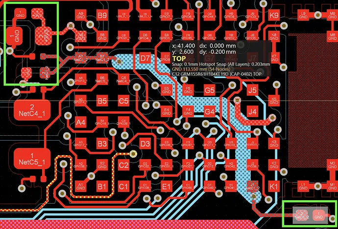
- Use vias to create physical barriers between analog and digital ground planes. This can be done by placing a row of ground vias along the boundary between the two sections, often referred to as a "via fence." This fence helps block EMI from crossing over.
- Avoid placing vias directly under high-speed digital components, as they can act as antennas and radiate noise. Instead, position vias at least 0.5 mm away from such components to minimize coupling.
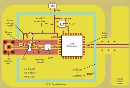
2. Optimize Ground Plane Connections with Vias
A solid ground plane is essential for noise reduction in mixed-signal PCBs, and through-hole vias play a key role in connecting ground layers. However, a common mistake is using a single, shared ground plane for both analog and digital circuits, which allows noise to propagate freely.
- Split your ground plane into separate analog and digital sections, connecting them at a single point (often near the power supply) using a via or a short trace. This "star grounding" technique prevents digital noise from contaminating the analog ground.
- Use multiple ground vias near power entry points to ensure a low-impedance path. For instance, placing 4-6 vias around a power connector can reduce voltage drops and stabilize the ground potential.
- Space ground vias evenly across the board to minimize ground loops. A spacing of 0.1 to 0.2 inches between vias is often recommended for high-frequency designs to maintain uniform grounding.
By carefully managing ground vias, you can achieve a cleaner signal environment and reduce interference significantly.
3. Minimize Via Inductance for High-Frequency Signals
Through-hole vias introduce inductance, which can cause signal degradation, especially in high-frequency digital circuits. High inductance can lead to ringing or overshoot, contributing to noise in mixed-signal systems. Here’s how to address this:
- Keep via lengths as short as possible by using thinner PCB stack-ups where feasible. A shorter via reduces its parasitic inductance, which can be critical for signals above 100 MHz.
- Use smaller via diameters for high-speed signals. A via diameter of 0.3 mm or less can lower inductance compared to larger 0.8 mm vias, though this must be balanced with manufacturing constraints.
- For critical signals, consider using multiple parallel vias to reduce the effective inductance. For example, two vias in parallel can cut inductance by nearly half compared to a single via.
These adjustments help maintain signal integrity and prevent noise from affecting both analog and digital components.
4. Manage Power Distribution with Vias
Power supply noise is a major concern in mixed-signal PCBs, as it can couple into both analog and digital circuits. Through-hole vias are often used to deliver power across layers, and their placement impacts voltage stability.
- Place power vias close to the pins of power-hungry components, such as microcontrollers or amplifiers, to minimize voltage drops. A distance of less than 0.1 inches is ideal for maintaining stable power delivery.
- Add decoupling capacitors near power vias to filter out high-frequency noise. A 0.1 μF capacitor placed within 0.05 inches of a power via can effectively suppress noise in the 10 MHz range.
- Use dedicated power planes for analog and digital sections, connecting them to the power source with separate vias. This prevents digital switching noise from affecting analog power lines.
Common Mistakes to Avoid in Through-Hole Via Design
Even with the best intentions, certain design errors can undermine your efforts to reduce noise and interference in mixed-signal PCBs. Here are some pitfalls to watch out for:
- Overcrowding Vias: Placing too many vias in a small area can weaken the PCB structure and increase parasitic capacitance, leading to signal crosstalk. Maintain a minimum spacing of 0.2 mm between vias to avoid this issue.
- Ignoring Layer Stack-Up: Routing high-speed signals through vias across multiple layers can introduce impedance mismatches. Plan your layer stack-up to minimize via transitions for critical signals, ideally keeping them on adjacent layers.
- Neglecting Thermal Effects: High-current vias can heat up, causing thermal noise that affects nearby analog circuits. Use larger via diameters (e.g., 0.6 mm or more) for power lines to handle current without overheating.
By steering clear of these mistakes, you can ensure that your through-hole vias contribute to a quieter, more reliable mixed-signal PCB design.
Advanced Tips for Via Design in High-Density Mixed-Signal PCBs
For complex or high-density designs, additional considerations can further enhance noise reduction and interference control. These advanced techniques are especially useful when working with compact boards or high-speed applications.
- Use Stitching Vias: Stitching vias are multiple ground vias placed around the perimeter of a PCB or between sections to maintain ground plane continuity across layers. They help suppress EMI and can be spaced at intervals of 1/20th of the wavelength of the highest frequency signal (e.g., 7.5 mm for a 1 GHz signal).
- Implement Back-Drilling: In high-speed designs, unused portions of through-hole vias can act as stubs, causing signal reflections. Back-drilling removes these stubs, reducing noise. This technique is particularly effective for signals above 500 MHz.
- Simulate Via Performance: Use PCB design software to simulate the electromagnetic behavior of vias before manufacturing. Tools can predict parasitic effects and help you adjust via size and placement for optimal performance.
These advanced methods require more planning and resources but can yield significant improvements in signal quality for demanding mixed-signal applications.
Conclusion: Building Cleaner Mixed-Signal PCBs with Via Design
Designing through-hole vias for mixed-signal PCBs is a powerful way to reduce noise and interference between analog and digital circuits. By focusing on strategic via placement, optimizing ground and power connections, minimizing inductance, and avoiding common mistakes, you can create a board that performs reliably under diverse conditions. Whether you’re working on a simple audio device or a complex IoT system, these principles will help you achieve better signal integrity and a quieter design.
Start by evaluating your current PCB layout and identifying areas where via design can be improved. Apply the tips and strategies shared in this guide, and consider advanced techniques like stitching vias or simulation for high-performance projects. With careful planning and attention to detail, your mixed-signal PCBs can deliver exceptional results, free from the disruptions of noise and interference.


