ALLPCB


Electrostatic Discharge (ESD) is a primary cause of overstress damage in electronic components and integrated circuit (IC) systems. Because the instantaneous voltage of an electrostatic event can be extremely high (often several thousand volts), the damage is typically destructive and permanent, leading to a complete circuit burnout. Preventing ESD damage is therefore a top priority in IC design and manufacturing.
Static electricity is often generated by human activity. Processes such as manufacturing, assembly, testing, storage, and handling can cause static charges to accumulate on people, instruments, or equipment. Even components themselves can accumulate a charge. When these charged objects come into contact with an IC, a discharge path is formed, causing immediate damage. This is why technicians historically wore anti-static wrist straps connected to the workbench when repairing computers—to prevent static from the human body from damaging chips. This phenomenon is analogous to lightning, where charge stored in clouds suddenly discharges through the atmosphere, a process that is more common during storms when high humidity creates a more conductive path.
While environmental controls like reducing friction, avoiding wool clothing, and managing air humidity can help mitigate static buildup at the source, this article will focus on implementing on-chip protection circuits. These circuits are designed to allow electronic components and systems to self-protect against external ESD events, much like a lightning rod protects a building.
Many IC design and manufacturing companies have dedicated teams focused on ESD. This article will explain the fundamental principles of ESD protection, covering concepts such as PN junctions, diodes, transistors, MOS devices, and snap-back behavior.
Circuit-Level ESD Protection
The PN junction diode is a foundational component for ESD protection. A diode exhibits forward conduction and reverse blocking characteristics. When the reverse bias voltage increases sufficiently, it enters avalanche breakdown and begins to conduct. A diode used in this way is called a clamp diode. This reverse-blocking behavior is ideal for ESD protection; the protection circuit remains inactive during normal operation but enters avalanche breakdown during an ESD event, creating a bypass path to protect the internal circuitry or gate. This is similar to an overflow drain in a sink, which prevents flooding if the faucet is left on.
A common question is whether the protection circuit is permanently destroyed after a breakdown event. The answer is generally no. PN junction breakdown can be categorized as either electrical or thermal. Electrical breakdown, which includes avalanche breakdown (in lightly doped junctions) and Zener breakdown (in heavily doped junctions), is caused by impact ionization creating new electron-hole pairs and is a recoverable process. Thermal breakdown, however, is non-recoverable, as the accumulated heat melts and destroys the silicon. To prevent thermal breakdown, the current during conduction must be limited, typically by placing a high-value resistor in series with the protection diode.
ESD protection structures are typically located near the chip's I/O pads, not deep within the internal circuitry. This placement ensures that external static charges are shunted away as quickly as possible, minimizing delay. It is common to see single-stage or even dual-stage ESD protection circuits on chip layouts for enhanced reliability. Additionally, silicide is often excluded from ESD protection areas to maintain a higher series resistance, which helps dissipate energy during an ESD event.
ESD Standards and Test Models
ESD testing is categorized into four main models based on the source of the static and the damage mode, but the first two are most commonly used in the industry.
- Human-Body Model (HBM)
- Machine Model (MM)
- Charged-Device Model (CDM)
- Field-Induced Model (FIM)
Human-Body Model (HBM)
HBM simulates a discharge from a charged person touching an IC pin. A common standard for HBM is MIL-STD-883C Method 3015.7, which defines an equivalent circuit of a 100pF capacitor in series with a 1.5kΩ resistor. Another relevant standard is EIA/JESD22-A114-A. According to MIL-STD-883C, devices are classified based on their failure threshold voltage: Class 1 (<2kV), Class 2 (2kV to 4kV), and Class 3 (4kV to 16kV).
Machine Model (MM)
MM simulates a discharge from a charged piece of automated equipment, such as a robotic arm, touching an IC pin. The standard EIA/JESD22-A115-A (or EIAJ-IC-121 Method 20) defines the equivalent circuit as a 100pF capacitor with a 0Ω resistor. Because metal equipment has virtually no resistance, the discharge time is extremely short (in the microsecond or millisecond range), and the resulting current is very high. Consequently, a 200V MM discharge can be more destructive than a 2kV HBM discharge. Furthermore, the presence of various conductors in machinery can introduce coupling effects, causing the discharge current to fluctuate over time.
ESD Test Procedure
The ESD test procedure is a step-stress test. A specified pin is subjected to an ESD pulse at a certain voltage. Afterward, the device's electrical characteristics are measured to check for damage. If no failure is detected, the ESD voltage is increased by a set step (e.g., 50V or 100V), and the process is repeated until failure occurs. The voltage at which the device fails is its ESD failure threshold. A typical test involves applying three "zaps" at each voltage level, often starting at 70% of the expected ESD threshold to reduce test time.
Pin Combination Test Methods
Since a chip has many pins, tests are performed using various pin combinations:
- I/O Pin Tests: Input and output pins are tested individually. This involves four combinations: positive and negative charges applied to an input pin (with other pins floating), and positive and negative charges applied to an output pin (with other pins floating).
- Pin-to-Pin Tests: Simulates a discharge between two pins. To simplify the vast number of possible pairs, a common method is to apply a positive or negative ESD voltage to one I/O pin while all other I/O pins are grounded, and the main power (Vdd) and ground (Vss) pins are left floating.
- Vdd-to-Vss Tests: Vdd and Vss pins are connected to the tester, and an ESD pulse is applied between them while all I/O pins are left floating.
- Analog Pin Tests: Analog circuits often use differential pairs or operational amplifiers with two inputs. To prevent failure of differential functionality, these input pairs are tested specifically, with all other pins floating.
ESD Implementation: Process vs. Design
As Moore's Law drives device dimensions smaller, with shallower junctions and thinner gate oxides (GOX), ICs become more susceptible to ESD. The introduction of silicide in advanced processes further exacerbates this vulnerability. ESD protection can be implemented at the foundry process level or through IC layout design.
Process-Level ESD Solutions
Foundry-level solutions involve modifying the PN junction or its load resistance.
- Source/Drain ESD Implant: Standard LDD (Lightly Doped Drain) structures have shallow junctions with sharp corners where the electric field can concentrate, making them vulnerable to ESD (<1kV). An alternative is to use a dedicated ESD implant to create a deeper N+ source/drain. This results in a rounded junction farther from the surface, significantly improving ESD performance (>4kV). However, this non-LDD device requires a longer gate to prevent punch-through and a separate SPICE model.
- Contact ESD Implant: A P+ boron implant is placed under the N+ drain contact, extending deeper than the N+ junction itself. This lowers the drain's breakdown voltage (e.g., from 8V to 6V), causing it to break down and conduct current before the more vulnerable LDD region fails. This method preserves the MOS structure and device dimensions, so no new SPICE model is needed. It is only suitable for non-silicide processes.
- Salicide Block (SAB): To lower interconnect resistance, modern processes use salicide. However, for an output driver, the resulting low resistance places the full ESD stress across the LDD and gate. A salicide block (SAB) mask is used to prevent salicide formation over the drain region of the protection device, increasing its series resistance. While this adds a photo layer and cost, it can improve ESD performance from ~1kV to >4kV.
- Series Resistor: A more cost-effective method is to intentionally add a series resistor (e.g., using an N-well resistor or a high-resistivity poly layer) to achieve a similar effect as the SAB method without an extra mask.
Layout-Level ESD Solutions
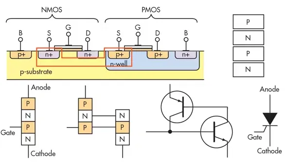
Design-level solutions rely on specific layout techniques. Many design rule manuals provide proven ESD solutions. The most common structures are the Gate-Grounded NMOS (GGNMOS) and Gate-Grounded PMOS (GGPMOS), where the gate, source, and bulk are shorted together, and the drain is connected to the I/O pad to absorb the ESD surge.
In a GGNMOS, the gate is off. During an ESD event, the high voltage at the drain causes the drain-to-bulk PN junction to undergo avalanche breakdown. The resulting large bulk current flows through the substrate resistance, creating a voltage drop that forward-biases the bulk-to-source junction. This activates the parasitic lateral NPN bipolar junction transistor (BJT), which enters its active region and exhibits snap-back behavior, shunting the ESD current safely to ground. A similar principle applies to PMOS devices.
The key design challenges are how to trigger the BJT reliably, how to sustain the snap-back characteristic, and how to achieve the target HBM rating (e.g., >2kV or >4kV). Reliable triggering requires a sufficiently large substrate current, which led to the development of the multi-finger layout structure. However, a major issue with multi-finger structures is non-uniform turn-on, where only a few fingers activate and conduct the majority of the current, limiting the overall effectiveness. Two techniques to address this are:
- Using a salicide-block (SAB) over the drain to create a high-resistance region, which helps distribute the ESD current more evenly across all fingers.
- Adding an inner pickup P-type ESD implant under the N+ drain to lower its avalanche breakdown voltage, triggering conduction earlier and with more current.
Two key points about snap-back based ESD protection:
- NMOS devices generally exhibit strong snap-back characteristics, while PMOS devices do not. This is because the charge carriers in NMOS breakdown are electrons, which have high mobility and generate a large substrate current (Isub) capable of turning on the parasitic BJT. This is much more difficult to achieve in PMOS. The general robustness of PMOS against ESD is often attributed to other factors, similar to its resilience to Hot Carrier Injection (HCI).
- The trigger voltage (Vt1) is the first knee-point of the snap-back I-V curve, corresponding to the breakdown voltage of the parasitic BJT. The holding voltage (Vh) is the minimum voltage required to keep the device in the snap-back state. It is critical to operate above Vh but avoid latch-up, which can lead to secondary (thermal) breakdown and permanent damage. The current at which this occurs (It2) must be limited, which can be done by controlling the device W/L ratio or increasing the drain contact-to-gate spacing.
Gate-Coupled (GC) ESD Technique
To overcome the non-uniform turn-on of multi-finger structures, the gate-coupled technique can be used. A capacitive coupling network applies a transient positive voltage to the gates of the protection transistors during an ESD event. This turns on the MOS channels before avalanche breakdown occurs, ensuring all fingers activate simultaneously and share the ESD current. This allows the full area of the protection device to be utilized effectively. However, a drawback of GCNMOS design is the risk of gate oxide breakdown due to the channel current, so careful design is required.
Silicon Controlled Rectifier (SCR) Protection
A more complex ESD protection structure is the Silicon Controlled Rectifier (SCR). It utilizes the parasitic PNPN structure inherent in CMOS technology. When triggered, this structure enters a latch-up state with a very low holding voltage, allowing it to shunt large amounts of current. An SCR can be designed by intentionally promoting the latch-up behavior that is normally suppressed in standard CMOS logic.
Conclusion
ESD protection is a multifaceted discipline involving a deep understanding of device physics, process technology, and circuit design. The primary protection strategies include resistive division, clamp diodes, MOS transistors, parasitic BJTs (snap-back), and SCRs. Effective ESD solutions require a co-design approach, considering factors at both the foundry process level and the IC layout level to ensure robust and reliable products.