ALLPCB


To achieve good electromagnetic compatibility (EMC) in high-speed backplane design, the printed circuit board must meet EMC and susceptibility standards during normal operation. A proper layer stackup is crucial for shielding and suppressing electromagnetic interference (EMI).
The EMC analysis of multilayer PCBs can be based on Kirchhoff's laws and Faraday's law of induction.
According to Kirchhoff's laws, any signal transmitted from a source to a load must have a path of least impedance. The signal current (I) and the image current (I') are equal in magnitude and opposite in direction. The layer where the image current (I') flows is called the image plane. If the layer beneath the signal trace is a power plane, the image current return path is achieved through capacitive coupling.
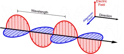
According to Faraday's law of induction:
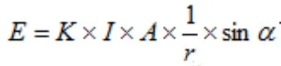
The larger the area A, the larger the value of E.
Based on these two laws, the following basic principles should be followed in multilayer PCB layer arrangement and stackup:
- The power plane should be as close as possible to the ground plane, and preferably located beneath the ground plane.
- Routing layers should be arranged adjacent to an image plane.
- The impedance between the power and ground planes should be minimized. The impedance Z0 is related to the distance D between the power and ground planes and the overlapping area W.
- Traces on internal layers form striplines, while traces on surface layers form microstrips, each with different characteristics.
Critical signal lines should be routed adjacent to a ground plane.
1. Six-Layer Board Stackups
| Layer 1 | Layer 2 | Layer 3 | Layer 4 | Layer 5 | Layer 6 | |
|---|---|---|---|---|---|---|
| A | S1 | GND | S2 | S3 | POWER | S4 |
| B | S1 | S2 | GND | POWER | S3 | S4 |
| C | S1 | GND | S2 | POWER | GND | S3 |
| D | GND | S1 | POWER | GND | S2 | GND |
For backplane designs, stackup D is recommended as it offers the best EMI performance for a six-layer board.
2. High-Speed Backplane Routing
Routing high-speed signals primarily involves managing signal integrity, including delay, reflection, crosstalk, simultaneous switching noise (SSN), and electromagnetic compatibility (EMI).
2.1 Clock Signal Lines
Clock signal lines require consideration of both signal integrity and EMI. Their proper handling is critical to the performance of a high-speed backplane.
In backplanes, clock signals are typically routed on inner layers, preferably between two plane layers. The impedance must be controlled, and consistency must be maintained when changing layers to prevent signal reflections from affecting the clock.
The spacing between clock lines and other traces should follow the 3W rule (center-to-center spacing is three times the trace width) to effectively prevent crosstalk. If there are synchronous timing requirements between signal lines, they should be routed with equal lengths to avoid timing issues caused by routing delays.
2.2 High-Speed Data Signal Lines
For high-speed signal lines, the main concerns are signal integrity issues such as impedance control, reflection, and crosstalk.
High-speed signals in backplanes are generally routed on inner layers adjacent to a ground plane. Impedance must be controlled and kept consistent across layer changes to prevent mismatches that can cause reflections, leading to overshoot and ringing that affect data reliability.
The spacing between high-speed signal lines and other traces should follow at least the 2W rule. If space allows, the 3W rule should be applied to effectively prevent crosstalk and ensure data reliability. Parallel data lines with synchronous timing requirements must be routed with identical lengths to prevent timing skew from routing delays.
2.3 LVDS Routing
Edge Rate: For multi-point backplane bus architectures, Time Domain Reflectometry (TDR) analysis is often used to describe the effect of the signal's edge rate. The signal's transition time (rise and fall time) is a critical parameter for transmission line calculations. It's important to note that multi-point and multi-drop bus structures are not suitable for signals with edge rates faster than 300 ps.
Stub Length: The impact of stub length on a backplane bus is also typically measured using TDR and Time Domain Transmission (TDT) methods. Generally, longer stubs introduce more severe impedance discontinuities on the line, which in turn cause larger damped oscillations on the signal's rising and falling edges. Therefore, shorter stubs on line cards have less impact on the backplane bus.
Placement of Interface Devices: To minimize the impact of stubs, their length should be kept as short as possible. During board layout, the position of interface devices should be determined first to ensure the shortest possible stub length. Bus transceivers (for multi-point) or receivers (for multi-drop) should be placed as close to the connector as possible, ideally using double-sided placement to reduce stub length.
Differential Impedance: BLVDS requires a differential impedance of 100 ohms between a pair of differential lines. If a spacing of 20 mils can be maintained between two differential pairs, their mutual common-mode and differential-mode interference can be considered negligible. The closer the traces of a differential pair are, the less they radiate, and the more external interference is converted to a common-mode signal at the receiver, which is beneficial. Let W be the trace width, d be the dielectric thickness, l be the spacing within a differential pair, and L be the spacing between pairs. A wider trace width (W) makes it easier to accurately manufacture the PCB's characteristic impedance; a trace width of 12 mils is common for backplanes. The dielectric thickness (d) should not be too small, as a smaller d results in lower characteristic impedance; the dielectric thickness between signal layers or between a signal layer and a ground plane on a backplane should not be less than 13 mils. The spacing (l) within a differential pair should be greater than d; if d is 13 mils, l should be at least 18 mils. The spacing (L) between differential pairs should generally be greater than twice the value of l.
Bus Termination: For a multi-point bus, termination resistors are required at both ends. For a multi-drop bus, one or two termination resistors are used depending on the driver's position. The resistor value should match the effective impedance of the loaded line. As a general rule, it's better to choose a termination resistance slightly higher than the actual effective impedance rather than lower. A higher value may only introduce unfavorable reflections, whereas a lower value can also cause a reduction in signal amplitude.
Stub Termination: For multi-drop connections, placing a series resistor of 15 to 30 ohms on each signal line of the LVDS differential pair near the connector pins can act as a filter for the edge rate. This effectively suppresses damped oscillations caused by stubs and fast edge rates. Alternatively, a small capacitor can be placed across the two inputs of the differential receiver, but its value is difficult to determine, so resistors are more commonly used. This technique is only suitable for multi-drop connections and is very effective when dealing with fast edge rates and long stubs.
Connector and Pin Assignment: The choice of connector depends on the application, with factors including the number of signal pins, mechanical dimensions, electrical performance, and pin arrangement. Generally, connectors with fewer pins per row are better. For most connectors, a differential pair should be placed within the same row to ensure equal trace lengths. Other TTL/CMOS signals should be separated from LVDS signals to avoid mutual interference. Use pins with special lengths for power and ground to ensure the correct power-up sequence, which is typically Ground, Power, then I/O. The power-down sequence is the reverse: I/O, Power, then Ground.
Pair Balancing: Imbalances in a differential pair introduce common-mode noise. The best way to control this is to keep the two lines of the pair as equal in length as possible, route them symmetrically, and maintain consistent spacing between them. Unequal lengths not only cause skew but also introduce jitter at the receiver. Additionally, avoid making the total length of a signal line an integer multiple of one-quarter of the signal's wavelength.
2.4 PCB Design Methodology Based on Signal Integrity Analysis
For high-speed backplane routing, a design methodology based on signal integrity (SI) analysis is recommended. The design flow is as follows:
- Before starting the PCB design, establish an SI model for high-speed digital signal transmission.
- Perform a series of pre-layout analyses based on the SI model. Use the simulation results to select appropriate component types, parameters, and circuit topologies as a basis for the circuit design.
- During the circuit design process, submit the design to the SI model for analysis. Calculate the design's solution space by considering tolerance ranges of components and the PCB, as well as possible variations in topology and parameters during layout.
- After the circuit design is complete, each high-speed digital signal should have a continuous and achievable solution space. This means that signal integrity requirements can still be met even with variations in PCB and component parameters and with some flexibility in component placement and trace routing.
- Before starting PCB layout, use the boundary values of each signal's solution space as constraints for placement and routing.
- During the PCB layout process, send partially or fully completed designs back to the SI model for post-layout analysis to confirm that the actual layout meets the expected SI requirements. If the simulation results are unsatisfactory, the layout or even the circuit design may need to be modified. This reduces the risk of product failure due to poor design.
- Once the PCB design is complete, the board can be fabricated. The tolerance range of the manufacturing parameters should be within the solution space identified by the SI analysis.
- After the PCB is manufactured, use instruments for measurement and debugging to verify the accuracy of the SI model and analysis, and use this feedback to refine the model.
- With an accurate SI model and analysis methodology, the PCB typically requires few or no revisions, which can shorten the product development cycle and reduce costs.
2.5 High-Speed Backplane Layout and Materials
High-speed backplane layout should follow the principles of separating analog and digital sections, as well as separating high-speed, medium-speed, and low-speed sections to prevent analog-digital interference and crosstalk between signals. Define multiple ground pins on the vertical pin headers of connectors to provide the shortest return path for signals and prevent crosstalk. The handling of analog and digital grounds on the backplane generally follows a "partitioned but not split" principle, where analog and digital signals are routed in their respective areas, and unrelated signal lines do not cross between these areas.