ALLPCB


Overview
A bipolar junction transistor (BJT) is commonly referred to as a transistor. In a broad sense there are many transistor types; in the narrow sense the term refers to the bipolar transistor, the most basic and widely used type. This article covers the bipolar transistor in the narrow sense.
Historical background
Before solid-state transistors, vacuum triodes were used in electronic circuits for amplification and switching. Vacuum tubes were bulky, power-hungry, and relatively slow. During World War II there was a need for a smaller, faster, and more reliable signal amplification device; research results emerged after the war. Early solid-state transistors used germanium because it was easier to obtain; after silicon became available and manufacturing processes matured, silicon devices largely replaced germanium. Over decades the variety of transistors expanded; small-signal devices typically use plastic packaging, while high-power devices often use metal or ceramic packages.
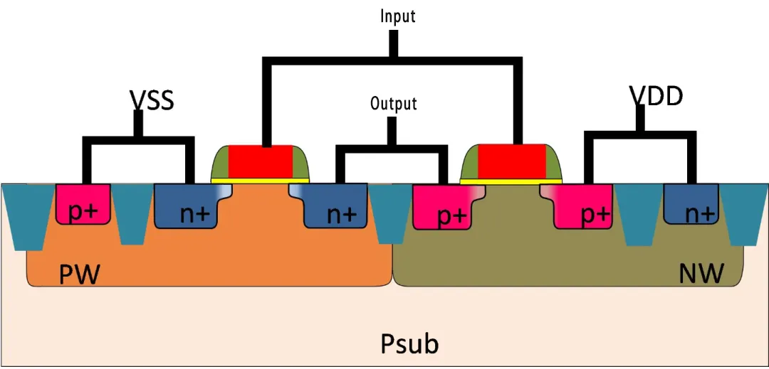
Core structure
A BJT consists of two back-to-back PN junctions and can be configured as NPN or PNP. The emitter region is heavily doped, the base is very thin, and the collector junction has a larger area.
Primary functions
Amplification: small changes in a small current produce larger changes in a larger current. Switching: a small current controls the on/off conduction of a larger current.
Operating states
A transistor is a device in which base current Ib controls the collector-emitter current Ic. Its behavior is analogous to a controllable valve. The transistor has four operating states: active (amplification), cutoff, saturation, and reverse-active.
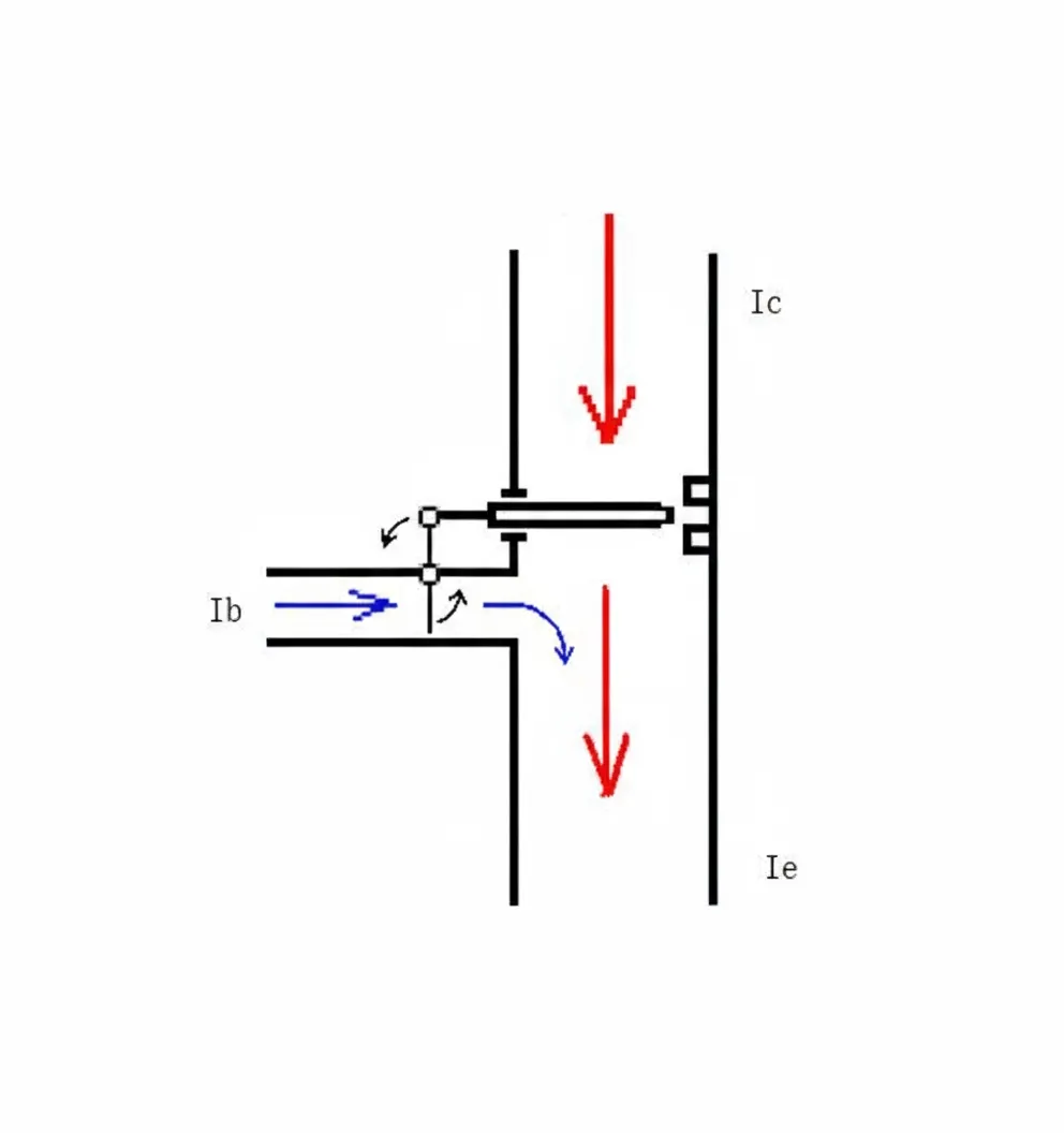
Collector/Base/Emitter current relationships
- IE = IB + IC
- IC = β * IB
- If IB = 0, then IE = IC = 0
For an NPN transistor, current enters through the base and collector and leaves through the emitter, i.e. IE = IB + IC.
If IB = 0, IC → 0 and the transistor is in cutoff, equivalent to an open switch. When IB > 0, small changes in IB produce amplified changes in IC by a factor of tens to hundreds. When IB becomes very large, IC saturates and no longer increases proportionally with IB; the transistor then behaves like a closed switch.
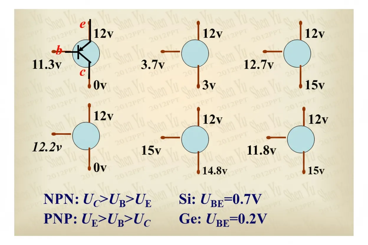
Collector/Base/Emitter voltage conditions
| Operating state | Emitter junction voltage Ube | Collector junction voltage Ubc |
|---|---|---|
| Active | Forward biased | Reverse biased |
| Cutoff | Reverse biased | Reverse biased |
| Saturation | Forward biased | Forward biased |
| Reverse-active | Reverse biased | Forward biased |
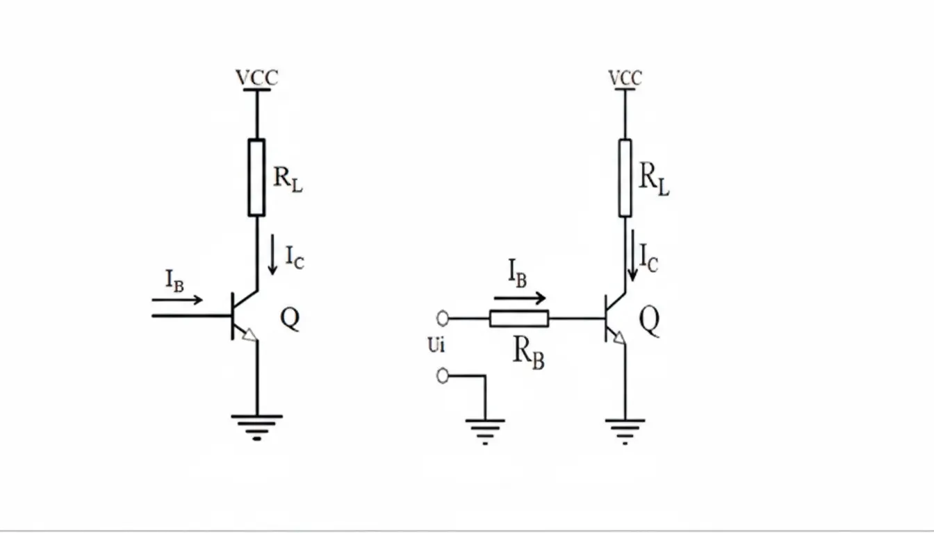
Note: In amplifier circuits IC = β * IB, where β is the current gain (typical range 100-1200). RL denotes the collector load resistor. In switching circuits (cutoff/saturation) avoid making IB excessively large to prevent damage to preceding stages or the transistor itself; RB is used as a base current limiting resistor.
Identification exercise
- Is the device silicon or germanium?
- What is the transistor part number?
- Which operating state is it in?