In the fast-evolving world of electronics, printed circuit board (PCB) rework is no longer just about fixing mistakes—it’s about precision, efficiency, and adapting to complex designs. If you’re searching for ways to master advanced rework techniques, leverage precision rework systems, or tackle challenges like fine pitch rework, multi-layer PCB rework, and automated optical inspection (AOI) rework, you’ve come to the right place. This guide dives deep into cutting-edge methods and tools that take PCB rework to the next level, ensuring high-quality results even in the most demanding projects.
Whether you’re an engineer working on intricate multi-layer boards or a manufacturer aiming to streamline rework processes, this blog will walk you through actionable strategies and technologies. Let’s explore how automation and precision can transform your PCB rework operations.
Why Advanced PCB Rework Matters in Modern Electronics
The electronics industry is pushing boundaries with smaller components, denser layouts, and more complex designs. As a result, traditional rework methods often fall short. Issues like damaged traces, misaligned fine-pitch components, or defects in multi-layer boards can lead to costly delays or product failures. Advanced rework techniques and automated systems address these challenges by improving accuracy, reducing human error, and speeding up the repair process.
Consider this: a single misplaced component on a board with 0.4mm pitch spacing can cause signal integrity issues, with impedance mismatches as high as 20% in high-speed designs operating at 5 GHz or more. Precision rework systems and automation help avoid such pitfalls, ensuring that reworked boards meet strict performance standards. Let’s break down the core areas where these advanced methods shine.
Exploring Advanced Rework Techniques for Modern Challenges
Advanced rework techniques go beyond basic soldering and desoldering. They involve specialized methods tailored to the intricacies of today’s PCBs. Here are some key approaches that engineers and manufacturers rely on:
1. Thermal Profiling for Component Safety
One of the biggest risks during rework is thermal damage to components or the board itself. Advanced rework techniques use precise thermal profiling to control heating and cooling cycles. By maintaining temperatures within a tight range—often between 220°C and 260°C for lead-free solder—engineers can prevent issues like pad lifting or component cracking. Modern rework stations often come with programmable profiles to match specific solder types and component sensitivities.
2. Non-Contact Soldering for Delicate Components
For boards with fragile or heat-sensitive parts, non-contact soldering methods like infrared (IR) or laser soldering are game-changers. These techniques focus heat only on the target area, minimizing the risk of overheating adjacent components. For instance, IR rework systems can achieve spot heating with a precision of ±2°C, ideal for dense boards where components are spaced less than 1mm apart.
3. Micro-Soldering for Fine Pitch Rework
Fine pitch rework is a critical skill when dealing with components that have lead spacing as small as 0.3mm. Micro-soldering, often done under a stereomicroscope with tips as fine as 0.2mm, allows technicians to work on these tiny connections without causing shorts or damage. Combining this with automated soldering systems can further enhance accuracy, reducing rework time by up to 30% on complex boards.
The Role of Precision Rework Systems in Automation
Manual rework is often too slow and error-prone for high-volume production or intricate designs. This is where precision rework systems step in, offering automated solutions that ensure consistency and quality. These systems integrate advanced hardware and software to handle everything from component removal to placement and soldering.
Key Features of Precision Rework Systems
Modern rework systems are equipped with features designed for accuracy and efficiency:
- High-Resolution Cameras: Built-in cameras with up to 1080p resolution provide clear visuals for aligning components with precision down to 0.01mm.
- Automated Placement: Robotic arms or pick-and-place mechanisms can position components with repeatability within ±0.02mm, crucial for fine-pitch applications.
- Integrated Heating Zones: Multi-zone heating ensures uniform temperature distribution, preventing thermal stress on boards with dimensions up to 500mm x 500mm.
These systems can reduce rework cycle times by as much as 40%, making them indispensable for manufacturers dealing with tight deadlines and high-quality standards.
Benefits for High-Volume Production
In high-volume settings, precision rework systems minimize downtime. For example, a fully automated system can process up to 50 boards per hour, compared to manual rework rates of just 5-10 boards in the same timeframe. This scalability is vital for industries like automotive or telecommunications, where even minor defects can lead to significant losses.
Tackling Multi-Layer PCB Rework Challenges
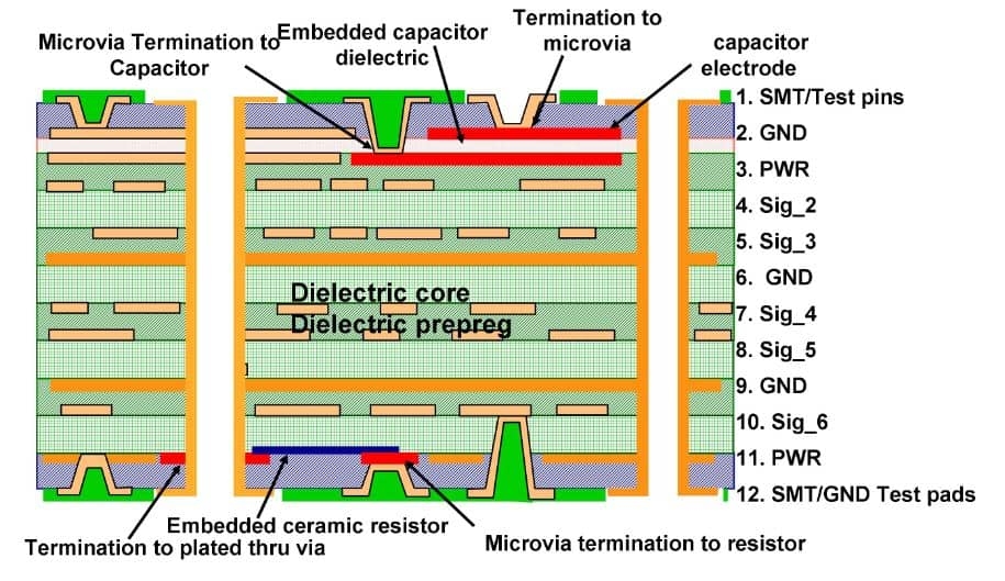
Multi-layer PCB rework presents unique challenges due to the complexity of internal layers and the risk of damaging hidden traces. Boards with 8 or more layers are common in advanced electronics, and rework errors can compromise signal integrity at frequencies above 1 GHz. Here’s how advanced techniques address these issues:
1. X-Ray Inspection for Hidden Defects
Before starting rework on multi-layer boards, identifying internal defects is crucial. X-ray inspection systems can detect issues like broken vias or misaligned internal traces with a resolution of 5 micrometers. This non-destructive method ensures that rework targets only the problematic areas without affecting the board’s structural integrity.
2. Controlled Depth Drilling
When accessing internal layers, controlled depth drilling allows technicians to remove material precisely, often within a tolerance of ±0.05mm. This technique prevents damage to adjacent layers and is often paired with real-time monitoring to stop drilling at the exact depth needed.
3. Via Repair and Reconstruction
Damaged vias in multi-layer boards can disrupt connectivity across layers. Advanced rework techniques involve micro-drilling to clean out damaged vias, followed by plating or filling with conductive epoxy. This restores connectivity while maintaining impedance values within 5% of the original design specifications.
Leveraging Automated Optical Inspection (AOI) for Rework
Automated optical inspection (AOI) rework is a powerful tool for identifying and correcting defects without human intervention. AOI systems use high-resolution cameras and machine learning algorithms to detect issues like misaligned components, solder defects, or missing parts with an accuracy rate of over 99%.
How AOI Enhances Rework Efficiency
AOI systems can scan a board in under 10 seconds, flagging defects for rework before they cause larger issues. For instance, in a board with 500 components, AOI can pinpoint a single misaligned part with a deviation as small as 0.1mm. This data is then fed into automated rework systems, which correct the issue without manual input, saving hours of troubleshooting time.
Integration with Rework Workflows
Many modern rework setups integrate AOI directly into the production line. After a defect is detected, the system generates a rework plan, specifying the exact location and type of correction needed. This closed-loop process ensures that rework is completed with minimal delay, often reducing overall production time by 25% in high-speed manufacturing environments.
Best Practices for Implementing Advanced Rework Techniques
To fully benefit from advanced rework techniques and systems, consider these practical tips:
- Invest in Training: Ensure your team is well-versed in using precision rework systems and AOI tools. Even a 1% error rate in fine-pitch rework can lead to significant rework costs.
- Choose the Right Equipment: Select rework systems that match your production needs. For multi-layer boards, prioritize systems with X-ray capabilities and multi-zone heating.
- Maintain a Clean Workspace: Contaminants like dust can cause defects during rework. Maintain a cleanroom environment with particulate control below 100 particles per cubic foot for critical projects.
- Monitor Performance Metrics: Track rework success rates and cycle times to identify areas for improvement. Aim for a first-pass yield of over 95% after rework.
Future Trends in Automated PCB Rework
The future of PCB rework lies in even greater automation and intelligence. Emerging technologies like artificial intelligence (AI) are being integrated into rework systems to predict defects before they occur, based on historical data and real-time monitoring. Additionally, advancements in 3D AOI are improving defect detection on complex geometries, achieving resolutions down to 1 micrometer.
Another trend is the rise of modular rework systems that can be customized for specific board types or production volumes. These systems reduce setup times by up to 50%, allowing manufacturers to adapt quickly to changing demands. Staying ahead of these trends will ensure your rework processes remain competitive in an increasingly complex industry.
Conclusion: Elevating PCB Rework with Advanced Techniques
Mastering advanced rework techniques and adopting precision rework systems are essential steps for anyone involved in PCB manufacturing or repair. From tackling fine pitch rework to managing multi-layer PCB rework and integrating automated optical inspection (AOI) rework, these methods offer the accuracy and efficiency needed to meet modern electronics standards.
By embracing automation and precision, you can reduce errors, save time, and ensure your boards perform reliably even under the most demanding conditions. Whether you’re refining thermal profiles or using X-ray inspection for multi-layer repairs, the tools and strategies discussed here provide a roadmap to success. Keep pushing the boundaries of what’s possible in PCB rework, and watch your projects thrive with unmatched quality.
 ALLPCB


