ALLPCB


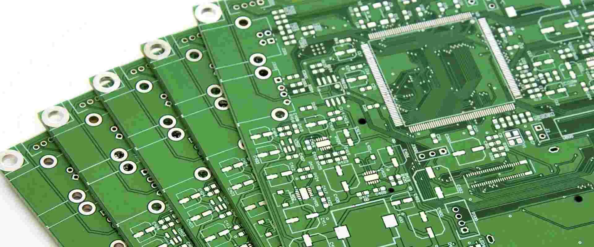
Ensuring high-quality plating on printed circuit boards (PCBs) is crucial for performance, reliability, and longevity. PCB plating quality directly impacts conductivity, corrosion resistance, and solderability. So, how can you maintain top-notch plating quality? The answer lies in strict quality control, regular maintenance, thorough inspection, and precise testing. In this comprehensive guide, we’ll dive into the best practices for maintaining PCB plating quality, covering every aspect from process control to advanced testing methods. Whether you’re an engineer or a manufacturer, these actionable tips will help you achieve flawless results.
Why PCB Plating Quality Matters
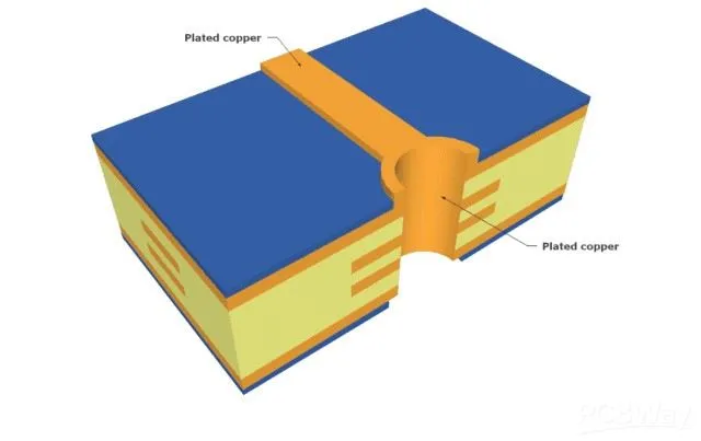
PCB plating serves as a protective and functional layer on the board’s surface and through-holes. It enhances electrical conductivity, prevents oxidation, and ensures proper soldering during assembly. Poor plating quality can lead to issues like weak solder joints, signal loss, or even complete board failure. For instance, inadequate copper plating thickness in through-holes can cause high resistance, leading to overheating or circuit breakdowns. Maintaining plating quality isn’t just about meeting standards—it’s about ensuring your PCBs perform reliably in real-world applications.
Understanding the PCB Plating Process
Before diving into maintenance and quality control, it’s important to understand the basics of PCB plating. The process typically involves depositing a thin layer of metal, such as copper, nickel, or gold, onto the board’s surface and inside vias or through-holes. The most common method is electroplating, where an electric current drives metal ions to bond with the PCB substrate. Another approach, electroless plating, is used for initial copper deposition in through-holes before electroplating.
Key factors in the plating process include bath chemistry, current density, and plating time. For example, a typical copper plating bath might aim for a thickness of 25-30 micrometers in through-holes, requiring precise control of current density (around 1.5-2.5 A/dm2) to avoid uneven deposition. Any deviation in these parameters can lead to defects like voids or insufficient thickness, which compromise quality.
Best Practices for Quality Control in PCB Plating
Quality control is the foundation of maintaining PCB plating excellence. Here are the best practices to implement during the manufacturing process:
1. Monitor Plating Bath Chemistry
The chemical composition of the plating bath must be consistent to ensure uniform metal deposition. Regularly test and adjust the levels of metal ions, additives, and pH. For copper plating, maintain a sulfuric acid concentration of 180-220 g/L and copper sulfate at 60-80 g/L. Use analytical tools like titration or spectroscopy to detect imbalances and prevent issues like rough plating or poor adhesion.
2. Control Current Density and Voltage
Uneven current distribution can cause over-plating in some areas and under-plating in others. Use rectifiers with precise controls to maintain a steady current density. For high-density interconnect (HDI) boards, lower current densities (around 1-1.5 A/dm2) may be needed to avoid burning or excessive deposition at edges.
3. Implement Process Automation
Automated plating systems reduce human error and ensure consistent results. These systems can monitor bath temperature (typically 20-30°C for copper plating) and agitate the solution to prevent ion depletion near the board surface. Automation also helps maintain uniform plating thickness, which is critical for meeting impedance requirements, such as 50 ohms for high-frequency signals.
Maintenance Tips for PCB Plating Equipment
Equipment maintenance is just as important as process control. Neglected tools and tanks can introduce contaminants or cause uneven plating. Follow these maintenance best practices:
1. Regular Cleaning of Plating Tanks
Residue and sludge buildup in plating tanks can contaminate the bath and affect plating quality. Schedule weekly cleaning to remove deposits and filter out impurities. Use deionized water for rinsing to avoid introducing minerals that could alter bath chemistry.
2. Inspect and Replace Anodes
Anodes in electroplating tanks degrade over time, leading to inconsistent metal ion release. Check anodes monthly and replace them if they show signs of excessive wear or pitting. For copper plating, using high-purity copper anodes (99.9% purity) ensures stable ion transfer.
3. Calibrate Monitoring Tools
Tools like pH meters, conductivity sensors, and current rectifiers need regular calibration to provide accurate readings. A miscalibrated sensor might report a pH of 2.0 when it’s actually 1.8, leading to improper bath adjustments. Calibrate equipment at least once a month or after major maintenance.
Inspection Techniques for PCB Plating Quality
Inspection is a critical step to catch defects early and ensure plating meets design specifications. Here are the most effective inspection methods:
1. Visual Inspection
Start with a basic visual check under magnification (10x-20x) to identify surface defects like roughness, discoloration, or incomplete coverage. This method is quick and can spot obvious issues, such as pinholes in gold plating over nickel layers, which might indicate poor adhesion.
2. Microsection Analysis
For a deeper look, perform microsectioning to examine the cross-section of plated through-holes. Use a metallographic microscope to measure plating thickness and check for voids or cracks. Industry standards often require a minimum copper thickness of 20 micrometers in through-holes for Class 2 boards and 25 micrometers for Class 3 boards.
3. Backlight Testing
Backlight testing helps assess the uniformity of copper plating in through-holes. By shining a light through the hole, you can detect thin or missing plating, which appears as brighter spots. This method is especially useful for multi-layer boards where hidden defects can cause failures.
Testing Methods to Validate PCB Plating Quality
Testing goes beyond visual checks to quantify plating performance. These methods ensure the plating can withstand environmental and operational stresses:
1. Thickness Measurement
Use tools like X-ray fluorescence (XRF) or coulometric testers to measure plating thickness non-destructively. For example, a surface copper layer should typically be 35-70 micrometers thick, depending on the board’s application. Consistent thickness ensures proper current-carrying capacity and impedance control.
2. Adhesion Testing
Adhesion tests, such as the tape test, verify that the plated layer won’t peel off under stress. Apply a piece of adhesive tape to the surface, press firmly, and pull it off quickly. If no metal comes off with the tape, the adhesion is satisfactory. Poor adhesion often results from surface contamination before plating.
3. Solderability Testing
Solderability is a key indicator of plating quality, especially for surface finishes like ENIG (Electroless Nickel Immersion Gold). Dip the board in molten solder (around 235°C) for 2-3 seconds and check if the plated areas are fully wetted. Incomplete wetting suggests oxidation or poor plating quality.
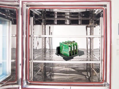
4. Environmental Stress Testing
Subject the board to thermal cycling (e.g., -40°C to 85°C for 100 cycles) or humidity exposure (85% RH at 85°C for 96 hours) to simulate real-world conditions. Inspect for delamination or corrosion in the plated layers. This test is critical for boards used in harsh environments, like automotive or aerospace applications.
Common PCB Plating Defects and How to Prevent Them
Even with strict controls, defects can occur. Here are common plating issues and prevention tips:
1. Pinholes and Voids
These are small gaps in the plated layer, often caused by gas bubbles or contamination. Prevent them by ensuring proper surface cleaning before plating and using agitation in the bath to release trapped gases.
2. Uneven Thickness
Uneven plating can result from improper current distribution or bath agitation. Use dummy boards or shielding to balance current flow across the PCB, and maintain consistent agitation speeds (e.g., 50-100 RPM for solution mixing).
3. Poor Adhesion
Adhesion failures often stem from inadequate surface preparation. Ensure thorough cleaning and micro-etching of the board surface to remove oxides and create a rough texture for better metal bonding.
Establishing a Quality Assurance System
Beyond individual practices, a robust quality assurance (QA) system ties everything together. Develop a checklist for each stage—pre-plating, plating, and post-plating—to ensure no step is overlooked. Train staff on proper procedures and use statistical process control (SPC) to track metrics like plating thickness or defect rates over time. For instance, aim for a defect rate below 1% per batch to meet high industry standards.
Additionally, comply with international standards like IPC-A-600 for PCB acceptability and IPC-6012 for performance specifications. These guidelines provide clear benchmarks for plating quality, such as minimum thickness and void allowances, ensuring your boards meet customer expectations.
Conclusion: Achieving Excellence in PCB Plating Quality
Maintaining PCB plating quality requires a multi-faceted approach that includes strict quality control, proactive maintenance, detailed inspection, and rigorous testing. By monitoring bath chemistry, calibrating equipment, and using advanced inspection techniques like microsection analysis, you can catch issues early and ensure consistent results. Implementing these best practices not only prevents costly rework but also builds trust with clients by delivering reliable, high-performing PCBs.
From controlling current density to conducting solderability tests, every step plays a vital role in achieving plating excellence. Start by reviewing your current processes, identifying gaps, and applying the tips outlined in this guide. With dedication to quality, your PCBs will stand up to the toughest demands, whether in consumer electronics, medical devices, or industrial systems.