 ALLPCB


In the world of PCB design, choosing the right via technology can make or break your project. When it comes to high-speed circuits and complex layouts, the debate often centers on backdrilling vs blind vias and backdrilling vs buried vias. So, what’s the difference, and which should you choose for optimal signal integrity and cost efficiency? In short, backdrilling removes unused portions of through-hole vias to improve signal integrity, blind vias connect an outer layer to an inner layer without going through the entire board, and buried vias connect internal layers without reaching the surface. Each has unique benefits and trade-offs in terms of performance and cost analysis.
In this detailed guide, we’ll break down these three via technologies, compare their applications in PCB design, and help you decide which is best for your needs. Whether you’re designing for high-speed data transfer or working with tight budgets, understanding these options is key to success.
What Are Vias in PCB Design?
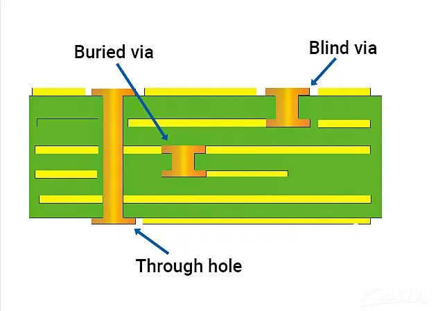
Vias are small conductive pathways that connect different layers of a printed circuit board (PCB). They allow signals and power to travel between layers, making multi-layer boards possible. Without vias, complex designs with dense routing would be nearly impossible. However, not all vias are created equal. The type of via you choose impacts signal integrity, board space, and manufacturing costs. Let’s explore the three via types in focus: backdrilled vias, blind vias, and buried vias.
Understanding Backdrilling in PCB Design
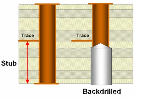
Backdrilling is a manufacturing technique used to improve signal integrity in high-speed PCB designs. It involves drilling out the unused portion of a through-hole via after the initial plating process. Why is this necessary? In high-speed circuits, the unused stub of a through-hole via can act like an antenna, causing signal reflections and degrading performance. By removing this stub, backdrilling minimizes these reflections and reduces noise.
For example, in a 10-layer PCB, a through-hole via might only need to connect layers 1 to 3. The remaining via length from layers 4 to 10 becomes a stub that can distort signals at frequencies above 5 GHz. Backdrilling removes this stub, ensuring cleaner signal transmission. This technique is especially critical for designs handling data rates of 10 Gbps or higher.
Advantages of Backdrilling
- Enhanced Signal Integrity: Reduces stub effects, lowering signal reflections and crosstalk.
- Cost-Effective for High-Speed Designs: Compared to other via types like blind or buried, backdrilling can be a more affordable way to achieve similar performance in some cases.
- Compatibility: Works with standard through-hole vias, making it adaptable to many designs.
Disadvantages of Backdrilling
- Manufacturing Complexity: Requires precise drilling equipment, which can increase production time.
- Not Space-Saving: Unlike blind or buried vias, backdrilling doesn’t free up surface space for component placement.
What Are Blind Vias and Their Role in PCB Design?
Blind vias connect an outer layer of a PCB to one or more internal layers without passing through the entire board. For instance, in a 6-layer PCB, a blind via might connect layer 1 (the top surface) to layer 2 or 3, stopping before reaching the bottom layer. This design saves space on the opposite side of the board and is often used in high-density interconnect (HDI) layouts.
Blind vias are ideal for compact designs where surface area is limited. They allow more routing flexibility on the outer layers since they don’t occupy space on both sides of the board. However, they require advanced manufacturing techniques, such as laser drilling for microvias, which can drive up costs.
Advantages of Blind Vias
- Space Efficiency: Frees up real estate on the opposite outer layer for components or traces.
- Signal Integrity: Shorter via lengths reduce signal distortion compared to full through-hole vias.
- Versatility: Commonly used in HDI designs for smartphones, tablets, and other compact devices.
Disadvantages of Blind Vias
- Higher Cost: Manufacturing blind vias, especially microvias, is more expensive due to specialized processes.
- Design Constraints: Requires careful planning to ensure proper layer connections without affecting other parts of the board.
Exploring Buried Vias in PCB Design
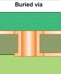
Buried vias are similar to blind vias but with one key difference: they connect only internal layers of a PCB without reaching either outer surface. For example, in an 8-layer board, a buried via might connect layers 3 to 5, remaining hidden beneath the surface. This makes buried vias invisible after assembly, freeing up space on both outer layers for components and routing.
Buried vias are often used in extremely dense designs where every bit of surface space matters. However, they are even more complex to manufacture than blind vias since they require sequential lamination processes during board fabrication.
Advantages of Buried Vias
- Maximum Space Savings: No surface exposure means both outer layers remain available for other uses.
- Improved Signal Integrity: Shorter internal connections reduce signal loss and interference.
- Ideal for HDI: Perfect for ultra-compact designs in advanced electronics.
Disadvantages of Buried Vias
- High Manufacturing Cost: Sequential lamination and precise drilling make buried vias expensive to produce.
- Testing Challenges: Since they’re hidden, inspecting or repairing buried vias is difficult.
Backdrilling vs Blind Vias: Key Differences
When comparing backdrilling vs blind vias, the choice often comes down to the specific needs of your design. Backdrilling focuses on improving signal integrity by eliminating via stubs in high-speed applications. Blind vias, on the other hand, prioritize space efficiency by limiting via penetration to specific layers.
For high-speed designs operating at frequencies above 5 GHz, backdrilling might be the better choice. It’s often less expensive than creating blind vias and can achieve similar signal performance by reducing reflections. However, if your design requires a compact layout with components on both sides, blind vias offer the space savings that backdrilling cannot provide.
In terms of cost analysis, backdrilling typically adds a moderate increase to manufacturing expenses due to the additional drilling step. Blind vias, especially when using laser-drilled microvias, can increase costs by 20-30% compared to standard through-hole vias, depending on the complexity of the design.
Backdrilling vs Buried Vias: A Detailed Comparison
The comparison of backdrilling vs buried vias reveals even starker contrasts. Backdrilling is primarily a signal integrity solution for through-hole vias, while buried vias are a space-saving technique for internal layer connections. If your primary concern is maintaining clean signals at data rates of 10 Gbps or more, backdrilling is likely the more practical and cost-effective option.
Buried vias shine in ultra-dense designs where surface space is at a premium. However, their manufacturing complexity can drive costs up significantly—sometimes by 30-50% more than standard vias—due to the need for multiple lamination cycles. Additionally, buried vias don’t directly address via stub issues in the same way backdrilling does, though their shorter lengths can still benefit signal integrity.
Signal Integrity: How These Via Types Compare
Signal integrity is a critical factor in modern PCB design, especially for high-speed applications like telecommunications, data centers, and automotive electronics. Let’s compare how these via types impact signal performance:
- Backdrilling: By removing via stubs, backdrilling can reduce signal reflections by up to 50% in high-speed designs, maintaining impedance control at levels like 50 ohms, which is common for high-frequency signals.
- Blind Vias: These vias improve signal integrity by shortening the signal path, reducing inductance and capacitance compared to through-hole vias. They’re effective for frequencies up to 10 GHz in many cases.
- Buried Vias: Similar to blind vias, buried vias offer shorter signal paths, minimizing distortion. However, their internal placement can make impedance matching more challenging without careful design.
For designs where signal integrity is the top priority, backdrilling often provides the most direct solution at a lower cost than blind or buried vias.
Cost Analysis: Which Via Type Fits Your Budget?
When it comes to cost analysis in PCB design, each via type has a different impact on your bottom line:
- Backdrilling: Adds a moderate cost increase, typically 10-20% more than standard through-hole vias, due to the additional drilling step. It’s often the most budget-friendly option for high-speed performance.
- Blind Vias: Can increase costs by 20-30% compared to through-hole vias, especially if microvias are involved. The price rises with the complexity of the layer stack-up.
- Buried Vias: The most expensive option, often costing 30-50% more than standard vias due to sequential lamination and precise manufacturing requirements.
If budget constraints are a major concern, backdrilling often strikes the best balance between cost and performance for high-speed applications. For compact, high-density designs, the added cost of blind or buried vias may be justified by the space savings they provide.
Choosing the Right Via for Your PCB Design
Deciding between backdrilling, blind vias, and buried vias depends on your project’s specific requirements:
- High-Speed Designs: If signal integrity at frequencies above 5 GHz is critical, backdrilling is often the most effective and affordable choice.
- Compact Layouts: For HDI designs where board space is limited, blind vias offer a good balance of space efficiency and performance.
- Ultra-Dense Designs: Buried vias are the go-to option when you need to maximize surface space on both sides of the board, despite their higher cost.
Consider factors like data rate, layer count, and budget when making your decision. For instance, a 12-layer PCB for a server application might benefit from backdrilling to handle 25 Gbps signals, while a 6-layer PCB for a wearable device might prioritize blind vias to save space.
Conclusion: Optimizing Your PCB Design with the Right Via Technology
In the battle of backdrilling vs blind vias and backdrilling vs buried vias, there’s no one-size-fits-all answer. Backdrilling excels in high-speed applications by enhancing signal integrity at a reasonable cost. Blind vias provide space savings for compact designs, while buried vias take density to the next level for the most intricate layouts. By understanding the strengths and weaknesses of each via type, you can make an informed decision that balances performance, space, and cost analysis.
At ALLPCB, we’re committed to helping you navigate the complexities of PCB design. Whether you’re optimizing for high-speed signals or tight layouts, our expertise and manufacturing capabilities ensure your project succeeds. Explore your via options today and elevate your next design to new heights.


