 ALLPCB


If you're wondering how copper weight affects your printed circuit board (PCB) performance, especially in terms of signal integrity, impedance control, and high-frequency applications, you're in the right place. At its core, copper weight—measured in ounces per square foot (oz/ft2)—determines the thickness of copper layers on a PCB and plays a critical role in how well your board handles electrical signals and power. Optimizing copper weight can improve signal clarity, reduce losses, and ensure reliable performance, particularly in demanding designs. In this blog, we’ll dive deep into the effects of copper weight on signal integrity, how to optimize it for impedance control, and its impact on high-frequency performance, providing actionable insights for your next project.
What Is Copper Weight in PCB Design?
Copper weight refers to the thickness of the copper layer on a PCB, typically measured in ounces per square foot. One ounce of copper (1 oz/ft2) translates to a thickness of about 1.37 mils (0.00137 inches or 35 micrometers). Common copper weights range from 0.5 oz to 3 oz for standard applications, though heavier options like 4 oz or more are used in high-power designs. This weight directly influences the board’s ability to carry current, manage heat, and maintain signal quality.
Understanding copper weight is the first step in optimizing PCB performance. A thicker copper layer (higher weight) can handle more current and dissipate heat better, but it may also affect signal behavior, especially at high frequencies. On the other hand, thinner copper (lower weight) is often used for finer traces in compact designs but might struggle with power demands or signal integrity. Let’s explore how these factors play out in real-world applications.

The Effect of Copper Weight on Signal Integrity
Signal integrity refers to the quality and reliability of electrical signals as they travel through a PCB. Issues like signal loss, crosstalk, and distortion can arise if the design isn’t optimized, and copper weight plays a significant role in this. Let’s break down how copper weight impacts signal integrity, especially when targeting the keyword “PCB copper weight effect on signal integrity.”
Thicker copper layers (higher weight, like 2 oz or 3 oz) reduce electrical resistance, which can help maintain signal strength over long traces. Lower resistance means less voltage drop and reduced signal attenuation, which is crucial for high-speed digital circuits. For instance, in a design operating at 5 GHz, a 1 oz copper layer might result in noticeable signal loss due to higher resistance, while a 2 oz layer could cut that loss by up to 20%, depending on trace length and layout.
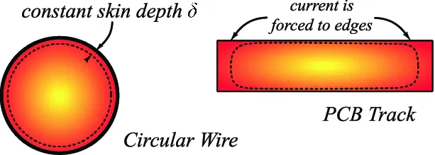
However, thicker copper isn’t always better. At high frequencies, signals travel along the surface of the conductor due to the skin effect—a phenomenon where current concentrates near the copper’s surface. If the copper is too thick, the inner portion of the trace isn’t utilized, wasting material and potentially increasing manufacturing costs without improving performance. Additionally, thicker copper can lead to uneven etching during fabrication, causing variations in trace width that disrupt signal integrity.
Thinner copper (like 0.5 oz or 1 oz) allows for finer traces and is often used in dense, high-speed designs. However, it comes with higher resistance, which can degrade signals over longer distances. Striking the right balance is key, and simulation tools can help predict how different copper weights affect signal behavior in your specific design.
Optimizing Copper Weight for Impedance Control
Impedance control is critical for ensuring that signals travel through a PCB without reflections or distortions, particularly in high-speed and high-frequency applications. When focusing on “optimizing copper weight for impedance control,” the thickness of the copper layer influences the characteristic impedance of a trace, which must match the system’s requirements (often 50 ohms for RF or 100 ohms for differential pairs).
The characteristic impedance of a trace depends on several factors: trace width, copper thickness, dielectric material, and the distance to the ground plane. Copper weight directly affects trace thickness, which alters the impedance. For example, a trace with 1 oz copper might have a width of 5 mils to achieve 50 ohms impedance on a standard FR-4 substrate with a 4-mil dielectric height. If you switch to 2 oz copper (twice as thick), the trace width must increase to around 6-7 mils to maintain the same impedance, assuming other factors remain constant. This adjustment can impact board layout, especially in tight spaces.
To optimize copper weight for impedance control, start by defining the target impedance for your design. Use an impedance calculator or simulation software to determine the ideal copper weight and trace dimensions. For most high-speed designs, 1 oz copper is a common choice because it balances manufacturability with performance. However, for applications requiring very precise impedance matching, such as RF circuits operating at 2.4 GHz, you might need to fine-tune the copper weight (e.g., 0.5 oz for thinner traces) and pair it with a controlled dielectric thickness.
Keep in mind that heavier copper weights can make impedance control more challenging during manufacturing. Thicker copper requires more precise etching to avoid over- or under-etching, which can skew trace dimensions and throw off impedance values. Working with a reliable fabrication partner ensures that tolerances are met, even with non-standard copper weights.
Copper Weight Impact on High-Frequency Performance
High-frequency designs, such as those for RF communication, 5G technology, or high-speed data transmission, are particularly sensitive to copper weight. When addressing “copper weight impact on high-frequency performance,” two main factors come into play: signal loss due to the skin effect and the interaction between copper thickness and dielectric properties.
As mentioned earlier, the skin effect causes high-frequency signals (above 1 GHz) to travel primarily on the surface of the copper trace. The skin depth—the distance over which the current density drops significantly—decreases as frequency increases. For example, at 1 GHz, the skin depth in copper is about 2.1 micrometers, much thinner than even a 0.5 oz copper layer (17.5 micrometers). This means that using copper thicker than necessary (e.g., 3 oz) provides little benefit for signal transmission and only adds cost and weight.
Moreover, the surface roughness of the copper can amplify signal loss at high frequencies. Rougher copper surfaces increase the effective path length for the signal, leading to higher losses. Many high-frequency designs use smoother copper finishes or thinner weights (like 0.5 oz or 1 oz) to minimize this effect. For instance, in a 10 GHz application, switching from a standard 1 oz copper with moderate roughness to a low-profile 1 oz copper can reduce insertion loss by up to 10-15%, depending on the trace length.
Another consideration is the interaction between copper weight and the dielectric material. Thicker copper can slightly alter the effective dielectric constant near the trace, impacting signal speed and phase. In high-frequency designs, this can lead to timing mismatches in differential pairs or phased arrays. Choosing the right copper weight, paired with a low-loss dielectric material, is essential for maintaining performance.
For most high-frequency applications, 1 oz copper is a safe starting point. If losses are too high, consider low-profile copper or thinner weights, and ensure your design accounts for skin effect limitations. Simulation tools can model these effects before fabrication, saving time and cost.
Practical Tips for Choosing the Right Copper Weight
Selecting the optimal copper weight for your PCB involves balancing performance, cost, and manufacturability. Here are some practical tips to guide your decision:
- Assess Current Requirements: For power-intensive designs, use heavier copper (2 oz or more) to handle higher currents and reduce heat buildup. A 2 oz copper layer can carry roughly twice the current of a 1 oz layer without overheating, based on standard IPC guidelines.
- Consider Signal Speed: For high-speed or high-frequency designs, stick to 1 oz or thinner copper to minimize skin effect losses and simplify impedance control.
- Evaluate Board Space: Thicker copper requires wider traces for the same impedance, which can be problematic in dense layouts. If space is limited, opt for thinner copper and adjust other parameters like dielectric thickness.
- Simulate Before Fabrication: Use design software to model how different copper weights affect signal integrity and impedance. This step can prevent costly redesigns.
- Consult Fabrication Limits: Not all manufacturers can handle extreme copper weights (like 4 oz or higher) without special processes. Confirm capabilities early in the design phase.
By tailoring copper weight to your specific application, you can avoid over-engineering (which increases cost) or under-engineering (which risks performance issues).
Common Challenges with Copper Weight Optimization
While optimizing copper weight offers clear benefits, it also comes with challenges. Manufacturing tolerances are tighter for non-standard weights, especially above 2 oz or below 0.5 oz. Variations in copper thickness can lead to inconsistent impedance or signal performance, particularly in high-frequency designs.
Thermal management is another concern. Heavier copper dissipates heat better, but it can also cause uneven thermal expansion during soldering, leading to warpage or delamination. Balancing copper weights across layers (e.g., using similar weights on top and bottom) can mitigate this issue.
Finally, cost is a factor. Heavier copper weights increase material and processing costs, while very thin copper may require advanced fabrication techniques. Weighing performance needs against budget constraints is essential for a successful design.
Conclusion: Mastering Copper Weight for Superior PCB Performance
Copper weight is a foundational element of PCB design that directly impacts signal integrity, impedance control, and high-frequency performance. By understanding the “PCB copper weight effect on signal integrity,” mastering “optimizing copper weight for impedance control,” and addressing the “copper weight impact on high-frequency performance,” you can unlock the full potential of your designs. Whether you’re working on a high-speed digital circuit, an RF application, or a power-heavy board, choosing the right copper weight—often starting with 1 oz as a baseline—ensures reliability and efficiency.
Remember to simulate your design, consider manufacturing constraints, and balance performance with cost. With these strategies, you’ll be well-equipped to create PCBs that meet the demands of modern electronics. Trust in expert fabrication services to bring your optimized designs to life with precision and quality.


