 ALLPCB


In the fast-evolving world of electronics, the push for smaller, faster, and more powerful devices has never been stronger. High-Density Interconnect (HDI) assembly techniques stand at the forefront of this revolution, enabling compact PCB designs that power everything from smartphones to medical devices. If you're looking to understand how HDI assembly miniaturization works and how it can transform your projects, you're in the right place. This blog dives deep into the core aspects of HDI technology, including microvia technology, fine-pitch component placement, HDI layer stacking, and compact PCB design strategies.
Whether you're an engineer, designer, or tech enthusiast, this guide will break down complex concepts into clear, actionable insights. Let's explore how HDI assembly techniques unlock the potential for miniaturization and high performance in modern electronics.
What is HDI Assembly and Why Does It Matter for Miniaturization?
HDI assembly refers to the process of creating printed circuit boards (PCBs) with a higher wiring density per unit area compared to traditional boards. This is achieved through advanced techniques that allow for more components to be packed into smaller spaces without sacrificing performance. Miniaturization, a key driver in industries like consumer electronics and automotive systems, relies heavily on HDI technology to meet the demand for lightweight, portable, and efficient devices.
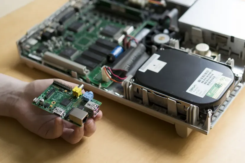
The significance of HDI assembly miniaturization lies in its ability to support complex designs in tiny footprints. For instance, modern smartphones often feature HDI PCBs with multiple layers and intricate connections, enabling them to house powerful processors, cameras, and sensors in a slim form factor. By leveraging HDI techniques, manufacturers can achieve up to 30% smaller board sizes compared to conventional designs, while also improving signal integrity and reducing power consumption.
Core HDI Assembly Techniques for Miniaturization
To truly understand HDI assembly miniaturization, we need to explore the specific techniques that make it possible. Below, we break down the key methods that enable compact PCB designs and high-performance electronics.
1. Microvia Technology: The Backbone of HDI Miniaturization
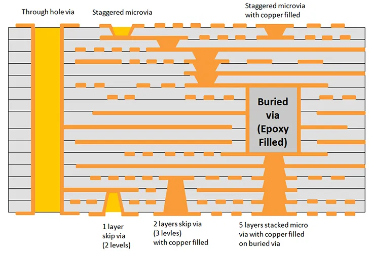
Microvia technology is a cornerstone of HDI assembly, allowing for the creation of tiny vias (holes) that connect different layers of a PCB. Unlike traditional through-hole vias, which can take up significant space, microvias are laser-drilled and have diameters as small as 0.1 mm (100 micrometers). This small size enables higher connection density, making it possible to stack more layers in a thinner board.
Microvias come in various forms, including blind vias (connecting an outer layer to an inner layer) and buried vias (connecting inner layers only). These configurations reduce the need for large drilled holes, freeing up space for additional traces and components. In practical terms, microvia technology can increase routing density by up to 50%, a critical factor for compact PCB design in devices like wearables and IoT gadgets.
Moreover, microvias improve signal integrity by shortening the path signals need to travel, reducing latency and electromagnetic interference (EMI). For high-speed applications, such as 5G devices, this can mean achieving signal speeds above 10 Gbps with impedance values tightly controlled at around 50 ohms.
2. Fine-Pitch Component Placement: Maximizing Space Efficiency
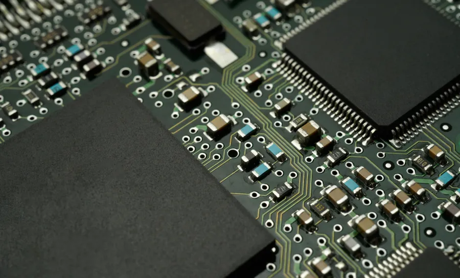
Fine-pitch component placement is another critical technique in HDI assembly miniaturization. It involves placing components with very small lead spacings—often less than 0.5 mm—closer together on the PCB. This is essential for fitting more functionality into smaller areas, a common requirement for modern electronics like tablets and smartwatches.
To achieve fine-pitch placement, HDI assembly often relies on advanced surface-mount technology (SMT) and automated pick-and-place machines. These tools ensure precision down to 0.01 mm, allowing for the accurate positioning of tiny components like 0201 or even 01005-sized resistors and capacitors. The result is a board that can support hundreds of components in a space smaller than a postage stamp.
However, fine-pitch placement requires careful design to avoid issues like solder bridging or thermal stress. Using high-quality solder masks and maintaining a pad-to-pad clearance of at least 0.1 mm can mitigate these risks, ensuring reliable performance in compact PCB designs.
3. HDI Layer Stacking: Building Up for Compact Designs
HDI layer stacking is the process of adding multiple layers to a PCB to increase its functionality without expanding its physical size. Traditional PCBs might have 4 to 6 layers, but HDI boards often feature 8, 10, or even 20 layers in the same or smaller footprint. This is made possible by using microvias to connect layers efficiently.
There are different stacking configurations in HDI assembly, such as 1+N+1 (one build-up layer on each side of a core) or 2+N+2 (two build-up layers on each side). These configurations allow designers to pack more circuitry into a thinner profile, often reducing board thickness to under 1 mm. For example, an HDI PCB with a 2+N+2 structure can achieve a wiring density of over 150 lines per square inch, compared to just 50 lines for a standard board.
Layer stacking also enhances thermal management and signal integrity by allowing for dedicated ground and power planes. This setup can reduce noise levels by up to 20 dB in high-frequency applications, making HDI layer stacking ideal for compact, high-performance designs.
4. Compact PCB Design: Bringing It All Together
Compact PCB design is the ultimate goal of HDI assembly miniaturization, combining microvia technology, fine-pitch placement, and layer stacking into a cohesive strategy. This approach focuses on optimizing every square millimeter of board space while maintaining functionality and reliability.
One key aspect of compact PCB design is the use of thinner materials, such as high-performance laminates with dielectric constants as low as 3.0. These materials support finer traces (down to 0.075 mm) and smaller spacings, enabling more connections in less space. Additionally, designers often employ sequential lamination processes to build up HDI layers, ensuring structural integrity despite the reduced thickness.
Another factor is the integration of embedded components, such as resistors and capacitors, directly into the PCB layers. This can reduce surface component count by up to 40%, further shrinking the board size. For instance, in medical devices like hearing aids, compact PCB design using HDI techniques can result in boards smaller than 10 mm x 10 mm, yet capable of handling complex signal processing.
Benefits of HDI Assembly Miniaturization for Modern Electronics
The adoption of HDI assembly techniques offers numerous advantages for industries striving to meet the demands of miniaturization and performance. Here are some of the key benefits:
- Smaller Form Factors: HDI technology enables up to 30-50% reduction in PCB size, crucial for portable devices like smartphones and wearables.
- Enhanced Performance: Shorter signal paths and reduced EMI improve speed and reliability, supporting applications with data rates exceeding 10 Gbps.
- Cost Efficiency in the Long Run: While initial design and manufacturing costs may be higher, the reduced material usage and improved product longevity can lower overall expenses.
- Greater Design Flexibility: With higher layer counts and denser routing, designers can innovate without being constrained by space limitations.
Challenges in HDI Assembly Miniaturization and How to Overcome Them
While HDI assembly offers incredible benefits, it also comes with challenges that designers and manufacturers must address to ensure success.
Design Complexity: HDI PCBs require precise planning to manage microvias, fine-pitch components, and multiple layers. Using advanced design software with simulation capabilities can help predict and resolve issues like signal crosstalk, which can occur at frequencies above 1 GHz.
Manufacturing Precision: The small tolerances in HDI assembly demand state-of-the-art equipment and strict quality control. For instance, laser drilling for microvias must maintain accuracy within 0.01 mm to avoid defects. Partnering with experienced manufacturers can ensure consistent results.
Thermal Management: Compact designs often generate more heat in a smaller area. Incorporating thermal vias and using materials with high thermal conductivity (above 1 W/mK) can help dissipate heat effectively.
Applications of HDI Assembly Miniaturization Across Industries
HDI assembly techniques are transforming a wide range of industries by enabling smaller, more efficient devices. Here are a few notable examples:
- Consumer Electronics: Smartphones, tablets, and wearables rely on HDI PCBs to pack advanced features into slim designs.
- Medical Devices: Miniaturized HDI boards power compact equipment like pacemakers and diagnostic tools, where space is critical.
- Automotive Systems: Advanced driver-assistance systems (ADAS) use HDI technology for reliable, space-efficient electronics.
- Aerospace: HDI assembly supports lightweight, high-performance avionics in constrained environments.
Future Trends in HDI Assembly Miniaturization
As technology continues to advance, HDI assembly techniques are evolving to meet even greater demands for miniaturization. Emerging trends include the use of ultra-thin materials with thicknesses below 0.05 mm, the integration of 3D stacking for even higher density, and the adoption of advanced manufacturing processes like additive printing for microvias. These innovations promise to push the boundaries of compact PCB design, enabling devices that are smaller and more powerful than ever before.
Conclusion: Embrace HDI Assembly for Next-Level Miniaturization
HDI assembly miniaturization is a game-changer for the electronics industry, offering the tools and techniques needed to create smaller, faster, and more efficient devices. By leveraging microvia technology, fine-pitch component placement, HDI layer stacking, and compact PCB design, engineers can overcome the challenges of limited space while delivering cutting-edge performance.
Whether you're designing the next generation of consumer gadgets or critical medical equipment, understanding and applying HDI assembly techniques can set your projects apart. With the right approach and partnerships, the possibilities for innovation are endless. Dive into the world of HDI technology today and unlock the full potential of miniaturization for your designs.


