 ALLPCB


In the fast-paced world of electronics, achieving high-speed performance is a top priority for engineers designing complex circuits. A 10-layer PCB stackup is often the go-to solution for applications requiring excellent signal integrity, precise impedance control, and robust power distribution. But what exactly makes a 10-layer PCB stackup so effective for high-speed designs? In this comprehensive guide, we’ll explore the intricacies of 10-layer PCB stackup design, focusing on impedance control, signal integrity, and material selection to help you unlock optimal performance for your projects.
Whether you’re working on telecommunications equipment, high-speed computing devices, or advanced medical systems, understanding how to design a 10-layer PCB stackup can make all the difference. Let’s dive into the details of crafting a stackup that meets the demands of modern electronics, ensuring your signals travel without distortion and your board performs reliably under pressure.
Why Choose a 10-Layer PCB Stackup for High-Speed Designs?
A 10-layer PCB stackup offers a perfect balance between complexity and functionality for advanced electronic applications. With multiple layers dedicated to signals, power, and ground planes, this configuration provides the flexibility needed to manage high-speed signals while minimizing interference. Unlike simpler 4 or 6-layer boards, a 10-layer design allows for better separation of critical signals, enhanced power distribution, and improved electromagnetic compatibility (EMC).
High-speed designs often operate at frequencies where signal integrity becomes a challenge. A well-designed 10-layer stackup addresses these challenges by providing dedicated layers for controlled impedance traces and reducing crosstalk between signals. Additionally, the increased layer count supports denser routing, making it ideal for compact devices with numerous components.
Key Benefits of a 10-Layer PCB Stackup
- Enhanced Signal Integrity: Multiple ground planes reduce noise and provide a stable reference for high-speed signals.
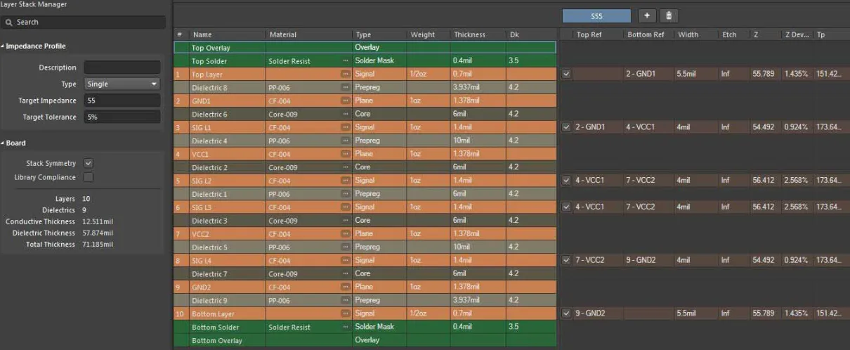
- Precise Impedance Control: Dedicated layers allow for consistent trace geometry, ensuring impedance matches target values like 50Ω for single-ended signals or 90Ω for differential pairs.
- Better Power Distribution: Separate power planes minimize voltage drops and ensure stable power delivery to components.
- Reduced EMI: Strategic layer arrangement shields sensitive signals from electromagnetic interference.
Designing a 10-Layer PCB Stackup for Impedance Control
Impedance control is a cornerstone of high-speed PCB design, especially in a 10-layer stackup. Without proper impedance matching, signals can reflect, leading to data loss or corruption. In a 10-layer PCB stackup, impedance control starts with careful layer arrangement and trace geometry to maintain consistent electrical characteristics across the board.
For instance, a common target impedance for high-speed digital signals is 50Ω for single-ended traces. Achieving this requires precise control over trace width, spacing, and the dielectric thickness between the trace and its reference plane. In a 10-layer stackup, you can dedicate specific layers to high-speed signals, placing them adjacent to ground planes to create a controlled impedance environment.
Steps to Achieve 10-Layer PCB Stackup Impedance Control
- Define Impedance Requirements: Identify the impedance values needed for your design, such as 50Ω for single-ended or 100Ω for differential signals.
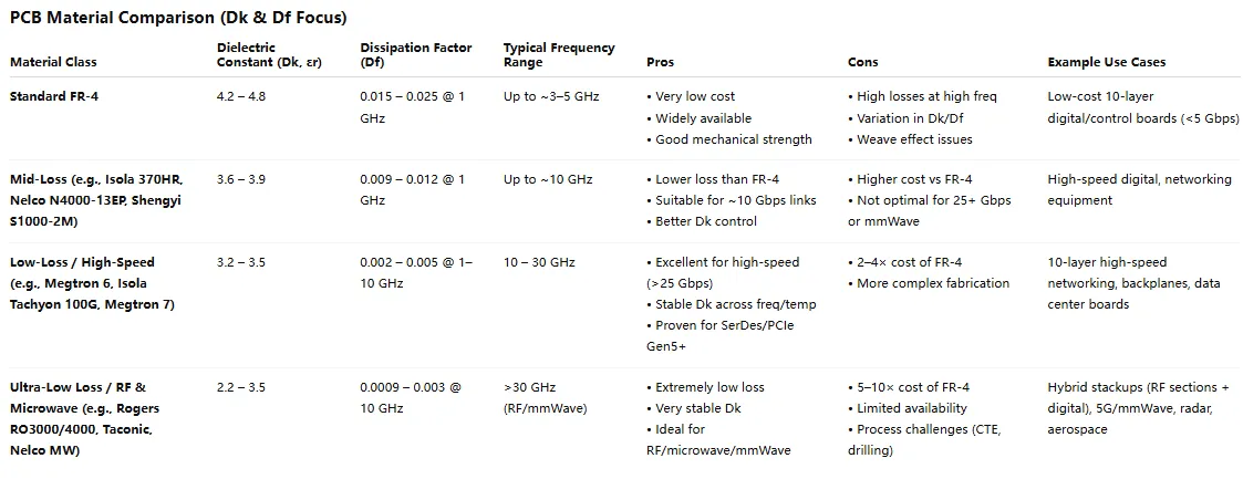
- Select Appropriate Materials: Use dielectric materials with a consistent dielectric constant (Dk) to avoid impedance variations. Common values range from 3.5 to 4.5 for standard FR-4 materials.
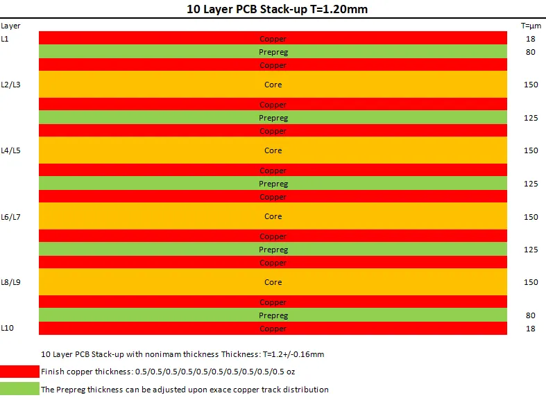
- Plan Layer Arrangement: Place signal layers next to ground planes to provide a stable reference and minimize loop inductance. For example, a typical 10-layer stackup might have signal layers on L1, L3, L8, and L10, with ground planes on L2, L4, L7, and L9.
- Calculate Trace Geometry: Use an impedance calculator to determine the trace width and spacing based on the dielectric thickness and material properties. For a 1.6mm thick board, a 50Ω trace might be around 6-8 mils wide on outer layers.
- Verify with Simulation: Use field solver tools to simulate impedance and make adjustments before fabrication.
By following these steps, you can ensure that your 10-layer PCB stackup meets the strict impedance requirements of high-speed applications, reducing signal reflections and ensuring reliable data transmission.
Ensuring Signal Integrity in a 10-Layer PCB Stackup
Signal integrity is the measure of how well a signal maintains its shape and timing as it travels through a PCB. In high-speed designs, factors like crosstalk, noise, and signal delay can degrade performance. A 10-layer PCB stackup offers unique advantages for maintaining signal integrity by providing ample space for shielding and routing optimization.
One of the primary strategies for ensuring 10-layer PCB stackup signal integrity is to use multiple ground planes. These planes act as shields, reducing crosstalk between adjacent signal layers and providing a low-impedance return path for high-speed signals. For example, placing a ground plane between two signal layers can reduce crosstalk by up to 20 dB compared to designs without such separation.
Tips for Optimizing Signal Integrity
- Minimize Via Transitions: Each via introduces inductance and can cause signal reflections. Route critical signals on a single layer when possible, or use back-drilling to remove unused via stubs.
- Use Differential Pairs: For high-speed signals, route differential pairs with consistent spacing (e.g., 5 mils apart for 100Ω impedance) to maintain signal balance.
- Avoid Routing Over Splits: Ensure that high-speed traces do not cross splits in power or ground planes, as this disrupts the return path and increases noise.
- Add Decoupling Capacitors: Place capacitors near power pins of high-speed components to stabilize voltage and reduce noise. A common value for high-speed designs is 0.1 μF.
By carefully planning your 10-layer PCB stackup with these principles, you can achieve clean, reliable signals even at frequencies exceeding 1 GHz, making your design suitable for applications like DDR4 memory or high-speed serial links.
Choosing the Right Materials for a 10-Layer PCB Stackup
Material selection plays a critical role in the performance of a 10-layer PCB stackup, especially for high-speed designs. The dielectric material between layers affects impedance, signal loss, and thermal stability, while the copper thickness impacts current-carrying capacity and trace resistance. Choosing the right materials for 10-layer PCB stackup materials ensures that your board can handle high frequencies and harsh operating conditions.
Key Material Considerations
- Dielectric Constant (Dk): A lower Dk value (e.g., 3.0-3.5) reduces signal propagation delay and loss, making materials like high-frequency laminates a good choice for designs above 5 GHz. Standard FR-4 with a Dk of 4.2-4.5 is suitable for lower frequencies.
- Dissipation Factor (Df): A lower Df (e.g., 0.002-0.005) minimizes signal loss at high frequencies. High-performance materials often outperform standard FR-4 (Df of 0.02) in this regard.
- Thermal Stability: Materials with a high glass transition temperature (Tg), such as 170°C or above, prevent delamination and warping during soldering or operation.
- Copper Weight: Use 1 oz copper (35 μm) for signal layers to balance manufacturability and performance. For power planes, 2 oz copper (70 μm) can handle higher currents without excessive heat buildup.
For most 10-layer PCB stackups, a hybrid approach combining standard FR-4 for inner layers and high-frequency materials for outer signal layers offers a cost-effective solution. This ensures that critical high-speed signals benefit from low-loss materials while keeping overall costs manageable.
Common 10-Layer PCB Stackup Configurations
While the exact arrangement of a 10-layer PCB stackup depends on the specific requirements of your design, there are several standard configurations that work well for high-speed applications. These configurations prioritize signal integrity, impedance control, and power distribution by strategically placing signal, ground, and power layers.
Example Configuration for High-Speed Design
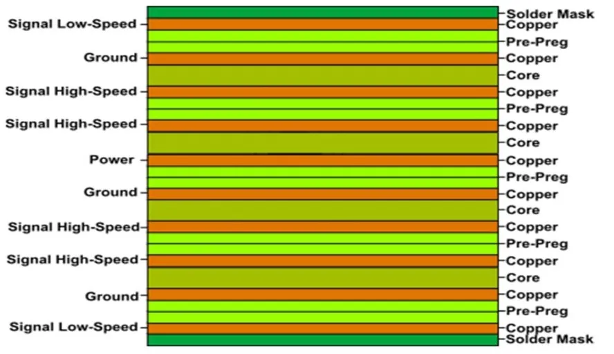
| Layer | Type | Purpose |
|---|---|---|
| L1 | Signal | Top layer for high-speed signals |
| L2 | Ground | Reference plane for L1 and L3 |
| L3 | Signal | Inner signal layer for routing |
| L4 | Ground | Shielding and reference plane |
| L5 | Power | Power distribution |
| L6 | Power | Secondary power plane |
| L7 | Ground | Reference plane for L6 and L8 |
| L8 | Signal | Inner signal layer for routing |
| L9 | Ground | Reference plane for L8 and L10 |
| L10 | Signal | Bottom layer for high-speed signals |
This configuration ensures that each signal layer is adjacent to a ground plane, providing a stable reference for impedance control and reducing crosstalk. Power planes are placed in the middle to minimize interference with signal layers while ensuring efficient power delivery.
Challenges and Solutions in 10-Layer PCB Stackup Design
Designing a 10-layer PCB stackup for high-speed performance comes with its share of challenges. From managing thermal dissipation to ensuring manufacturability, engineers must address several factors to create a reliable board.
Common Challenges
- Thermal Management: High-speed components generate significant heat, which can cause warping or delamination in a multi-layer board.
- Manufacturing Tolerances: Small variations in dielectric thickness or trace width can affect impedance, especially in high-frequency designs.
- Cost Constraints: Advanced materials and complex stackups increase fabrication costs, which may not be feasible for all projects.
Practical Solutions
- Use Thermal Vias: Add vias near heat-generating components to transfer heat to inner layers or external heatsinks.
- Work with Fabricators Early: Collaborate with your manufacturing partner to define achievable tolerances and adjust your design accordingly.
- Optimize Material Selection: Balance performance and cost by using high-performance materials only where necessary, such as for outer signal layers.
By anticipating these challenges and implementing targeted solutions, you can create a 10-layer PCB stackup that performs reliably without exceeding budget constraints.
Conclusion: Mastering 10-Layer PCB Stackup Design for High-Speed Success
A well-designed 10-layer PCB stackup is a powerful tool for achieving high-speed performance in modern electronics. By focusing on impedance control, signal integrity, and material selection, you can create a board that meets the demands of even the most complex applications. Whether you’re routing high-speed signals for a data center or designing a compact device with tight spacing, the principles outlined in this guide will help you unlock the full potential of your 10-layer PCB stackup.
From carefully arranging layers to selecting the right materials, every decision in the design process impacts the final performance of your board. Take the time to simulate, test, and refine your stackup, and you’ll be rewarded with a design that delivers clean signals, stable power, and long-term reliability. With these insights, you’re well-equipped to tackle the challenges of high-speed PCB design and bring your innovative ideas to life.


