 ALLPCB


High-layer-count PCB manufacturing is a complex process often used in advanced electronics like telecommunications, aerospace, and medical devices. These PCBs, typically with 8 or more layers, are essential for compact, high-performance designs. However, their complexity introduces unique challenges, such as manufacturing defects, layer alignment issues, and via reliability problems. In this comprehensive guide, we’ll explore these common issues and provide actionable solutions to help engineers and manufacturers overcome them. Whether you’re dealing with signal integrity problems or fabrication errors, this blog will equip you with the knowledge to troubleshoot effectively.
What Are High-Layer-Count PCBs and Why Do Issues Occur?
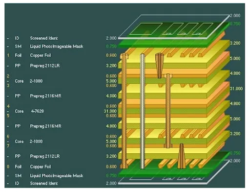
High-layer-count PCBs are printed circuit boards with multiple conductive layers stacked together, often exceeding 8, 12, or even 20 layers in sophisticated applications. These boards enable intricate circuit designs, high-density interconnects, and efficient power distribution. They are widely used in servers, high-speed communication devices, and industrial control systems where space and performance are critical.
However, the increased number of layers amplifies the risk of manufacturing defects. Each additional layer introduces new variables, such as alignment precision, material stress, and thermal expansion differences. Issues like PCB layer alignment errors can lead to signal crosstalk, while via reliability problems can cause intermittent connections or complete failures. Understanding the root causes of these challenges is the first step to resolving them.
Common Defects in High-Layer-Count PCB Manufacturing
Manufacturing defects in high-layer-count PCBs can significantly impact performance and reliability. Below, we dive into the most frequent issues, their causes, and how to address them.
1. PCB Layer Alignment Issues
Layer alignment, or registration, is critical in multi-layer PCBs. Misalignment occurs when the layers of a PCB do not stack precisely, leading to mismatched vias, traces, and pads. Even a small deviation of 0.1 mm can disrupt signal paths or cause short circuits, especially in high-density designs.
Causes:
- Inaccurate drilling or imaging during fabrication.
- Thermal expansion or contraction of materials during lamination, often due to mismatched coefficients of thermal expansion (CTE) between layers.
- Improper handling or storage leading to material warpage.
Solutions:
- Use advanced optical alignment systems during fabrication to ensure precision within tolerances of ±0.05 mm.
- Select materials with similar CTE values to minimize thermal stress. For example, FR-4 and high-Tg materials should be matched carefully.
- Implement strict quality control checks, such as X-ray inspection, to detect misalignments early in the process.
2. Via Reliability Problems
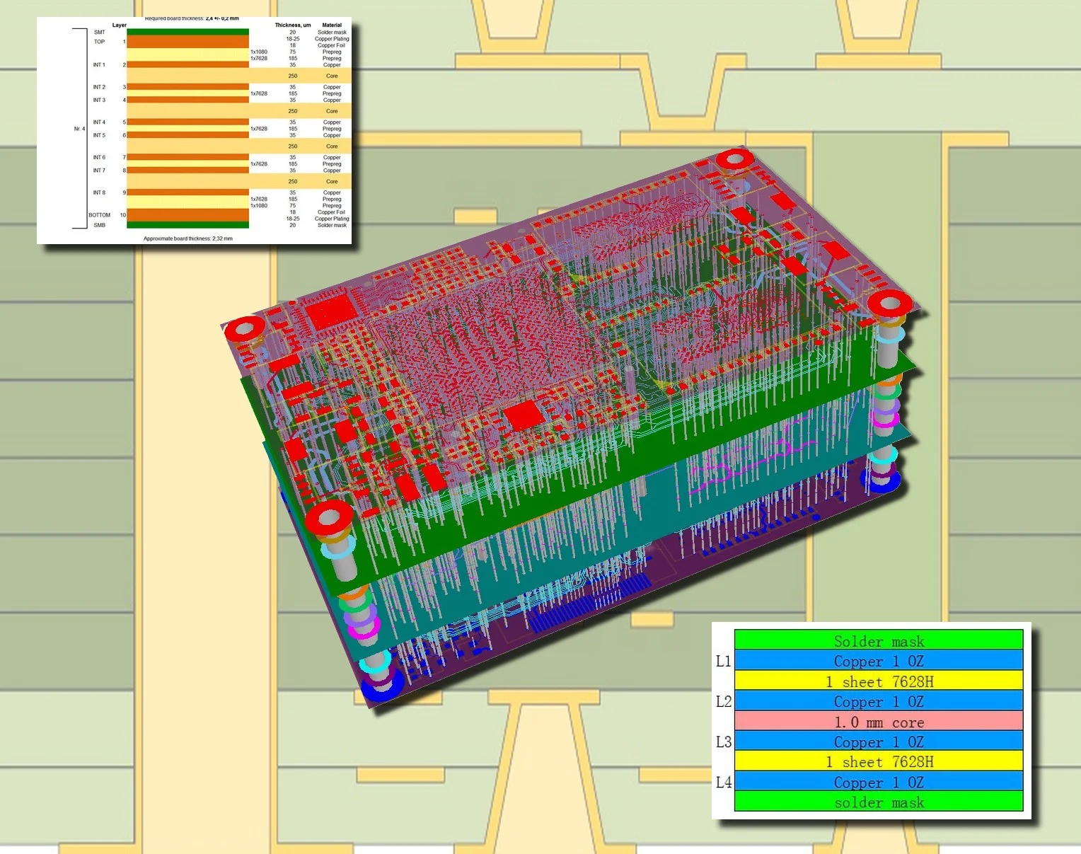
Vias are tiny holes that connect different layers of a PCB, and their reliability is crucial for signal and power transmission. In high-layer-count PCBs, vias are more prone to failure due to increased drilling depth and aspect ratios (depth-to-diameter ratio) as high as 10:1 or more.
Causes:
- Poor plating quality, leading to insufficient copper thickness inside the via walls (target thickness is typically 20-25 micrometers).
- Thermal stress during soldering or operation, causing via barrel cracks.
- High aspect ratios making it difficult to achieve uniform plating or resin fill in blind and buried vias.
Solutions:
- Opt for sequential lamination processes to reduce stress on vias in high-layer-count designs.
- Ensure proper via filling with conductive or non-conductive epoxy to prevent voids and enhance structural integrity.
- Conduct thermal cycling tests (e.g., -40°C to 125°C for 1000 cycles) to validate via reliability under stress.
3. Delamination and Blistering
Delamination refers to the separation of layers within a PCB, while blistering appears as bubbles or raised areas on the surface. Both defects weaken the board’s structural integrity and can disrupt electrical performance.
Causes:
- Moisture absorption during storage or processing, leading to vapor pressure buildup during soldering.
- Inadequate bonding between layers due to poor resin flow or insufficient curing.
- Thermal mismatches during high-temperature processes like reflow soldering at 260°C.
Solutions:
- Store materials in controlled environments (humidity below 50%) and use moisture barrier bags.
- Optimize lamination parameters, such as pressure (300-500 psi) and temperature (180-200°C), to ensure proper bonding.
- Bake PCBs before assembly to remove trapped moisture, typically at 120°C for 2-4 hours.
Signal Integrity Challenges in High-Layer-Count PCBs
Beyond physical defects, high-layer-count PCBs often face signal integrity issues due to their complex design. These problems can degrade performance, especially in high-speed applications where data rates exceed 10 Gbps.
1. Crosstalk and Electromagnetic Interference (EMI)
Crosstalk happens when signals from adjacent traces or layers interfere with each other, often due to tight spacing in high-density designs. EMI can also disrupt signals, especially in boards with mixed analog and digital circuits.
Causes:
- Inadequate spacing between traces, often less than 0.2 mm in high-density areas.
- Poor grounding or lack of shielding layers in the stack-up design.
- Impedance mismatches, deviating from the target value (e.g., 50 ohms for high-speed signals).
Solutions:
- Increase trace spacing where possible or use guard traces to isolate high-speed signals.
- Design stack-ups with dedicated ground planes to minimize EMI and maintain controlled impedance.
- Use simulation tools to model and adjust impedance values during the design phase, targeting a tolerance of ±10%.
2. Signal Loss and Attenuation
Signal loss becomes more pronounced in high-layer-count PCBs due to longer trace lengths and dielectric losses in materials at high frequencies (above 1 GHz).
Causes:
- Use of standard FR-4 material with a high dissipation factor (Df) of around 0.02, unsuitable for high-frequency signals.
- Long vias or traces increasing resistance and inductance.
- Skin effect at high frequencies, where current flows only on the surface of conductors.
Solutions:
- Switch to low-loss dielectric materials with a Df below 0.005 for high-speed designs.
- Minimize via stub lengths to reduce parasitic inductance, ideally keeping stubs below 0.3 mm.
- Optimize trace widths and copper thickness (e.g., 1 oz copper for power traces) to mitigate skin effect losses.
Best Practices for Preventing High-Layer-Count PCB Manufacturing Defects
While troubleshooting is essential, prevention is always better than repair. Here are proven strategies to minimize issues during the design and manufacturing stages.
1. Collaborate Early with Manufacturers
Engage with your fabrication partner during the design phase to understand their capabilities and limitations. For instance, confirm their ability to handle high aspect ratio vias or specific material requirements. This collaboration can prevent costly redesigns or delays.
2. Implement Design for Manufacturability (DFM) Guidelines
DFM ensures your design aligns with manufacturing constraints. Key practices include maintaining minimum drill sizes (e.g., 0.2 mm for microvias), adhering to annular ring requirements (minimum 0.15 mm), and avoiding overly tight tolerances unless necessary.
3. Conduct Thorough Testing and Inspection
Use advanced testing methods to catch defects early. Automated Optical Inspection (AOI) can detect surface-level issues, while microsectioning and X-ray analysis reveal internal defects like via cracks or layer misalignments. Electrical testing, such as flying probe or in-circuit testing, ensures functionality before assembly.
How to Troubleshoot High-Layer-Count PCB Issues Effectively
When defects or performance issues arise, a systematic troubleshooting approach can save time and resources. Follow these steps to identify and resolve problems.
1. Visual and Physical Inspection
Start with a detailed visual check for obvious defects like delamination, burns, or misaligned components. Use a magnifying glass or microscope for finer details, especially around vias and solder joints.
2. Electrical Testing for Signal Issues
Use a multimeter or oscilloscope to measure continuity, resistance, and signal integrity. For high-speed designs, Time Domain Reflectometry (TDR) can pinpoint impedance discontinuities with a resolution of ±1 ohm.
3. Thermal Imaging for Hotspots
Thermal cameras can detect overheating areas caused by poor power distribution or short circuits. Hotspots above 85°C often indicate underlying issues like insufficient copper thickness or via failures.
4. Root Cause Analysis
Once an issue is identified, trace it back to its source. Was it a design flaw, material choice, or fabrication error? Document findings to prevent recurrence in future projects.

Conclusion: Mastering High-Layer-Count PCB Manufacturing
High-layer-count PCB manufacturing comes with unique challenges, from layer alignment issues to via reliability problems and signal integrity concerns. By understanding these common defects and implementing the solutions outlined in this guide, engineers and manufacturers can achieve higher yields and better performance. Prevention through careful design, material selection, and collaboration with fabrication partners is key, but effective troubleshooting ensures issues are resolved quickly when they arise.
With the right strategies, you can navigate the complexities of high-layer-count PCBs and deliver reliable, high-quality products for even the most demanding applications. Stay proactive, test thoroughly, and keep refining your processes to stay ahead in this ever-evolving field.


