ALLPCB


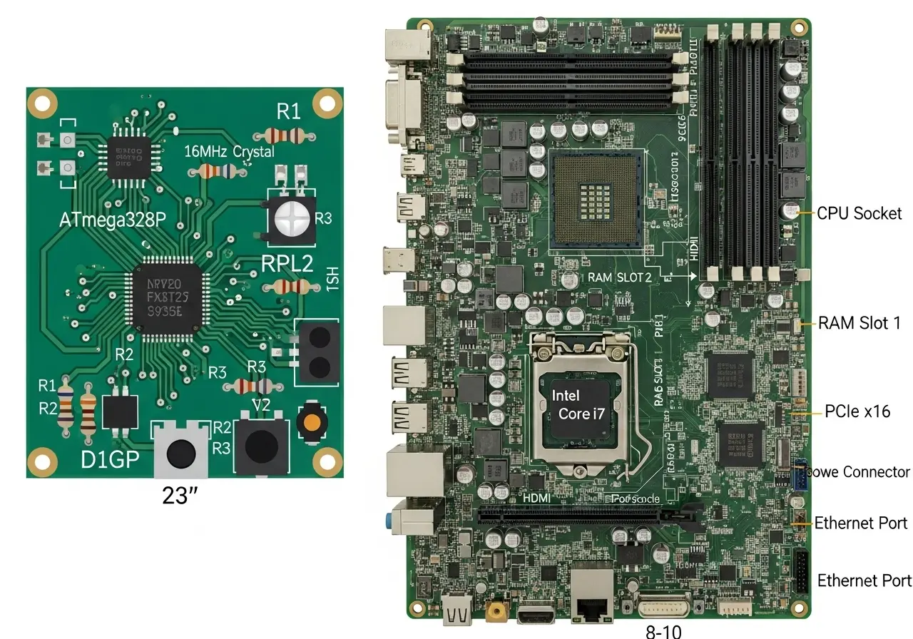
In high-speed digital circuits, the size of a printed circuit board (PCB) plays a critical role in maintaining signal integrity. Smaller PCBs, often used in compact devices, can introduce challenges like signal reflection, impedance mismatches, and crosstalk, while larger PCBs may face issues with signal delay and material costs. Understanding how PCB size impacts signal integrity is essential for designing reliable, high-performance electronics. In this blog, we’ll dive deep into these effects, covering topics like PCB size and signal reflection, impedance control in small PCBs, crosstalk reduction in compact layouts, signal integrity simulation for custom PCB sizes, and PCB material selection for high-speed miniaturization. Let’s explore how to optimize your designs for better performance.
Why PCB Size Matters for Signal Integrity
Signal integrity refers to the quality of an electrical signal as it travels through a PCB. In high-speed digital circuits, where data rates often exceed 1 Gbps, even small distortions can lead to errors or system failures. PCB size directly influences factors like trace length, component placement, and electromagnetic interference (EMI), all of which affect how signals behave. For instance, a smaller PCB might force shorter traces, but it can also lead to tighter spacing, increasing the risk of crosstalk. On the other hand, larger PCBs allow for better spacing but may introduce longer traces that cause signal delays.
Balancing these trade-offs is key to successful design. By carefully considering PCB size, engineers can minimize issues and ensure reliable performance in high-speed applications like telecommunications, computing, and consumer electronics.
PCB Size and Signal Reflection: A Hidden Challenge
Signal reflection occurs when a signal encounters an impedance mismatch along its path, causing part of the signal to bounce back toward the source. This can distort the signal and lead to errors in high-speed digital circuits. PCB size has a direct impact on signal reflection, especially in smaller boards where trace lengths and terminations are harder to control.
In a compact PCB, shorter traces might seem beneficial for reducing delay, but they can create problems if not matched properly with the load. For example, a trace that’s too short might not allow enough space for proper termination resistors, leading to reflections. A common rule of thumb is that signal reflection becomes significant when the trace length exceeds 1/6th of the signal’s wavelength. For a 5 GHz signal, this wavelength is about 60 mm in a typical dielectric material with a velocity factor of 0.5, meaning traces longer than 10 mm need careful attention.
To mitigate signal reflection in smaller PCBs, engineers must focus on precise trace routing and termination techniques. Using simulation tools to model signal behavior before fabrication can also help identify potential issues early in the design process.
Impedance Control in Small PCBs: Precision is Key
Impedance control is vital for maintaining signal integrity, as it ensures that the signal travels through the PCB without significant loss or distortion. In small PCBs, achieving impedance control is challenging due to limited space for trace width adjustments and layer stack-up configurations. A typical target impedance for high-speed digital signals is 50 ohms for single-ended traces or 100 ohms for differential pairs, but deviations as small as 10% can cause noticeable signal degradation.
In compact designs, narrower traces are often necessary to fit within the limited board area. However, narrower traces increase resistance and can alter impedance if not paired with the right dielectric thickness. For example, a trace width of 5 mils (0.127 mm) on a standard FR-4 material with a dielectric constant of 4.2 might require a specific height above the ground plane to maintain 50-ohm impedance. Reducing board size without adjusting these parameters can disrupt the balance, leading to signal loss.
To achieve impedance control in small PCBs, designers should prioritize consistent trace widths, use controlled dielectric materials, and consider microstrip or stripline configurations. Working with advanced fabrication processes that ensure tight tolerances can also make a big difference.
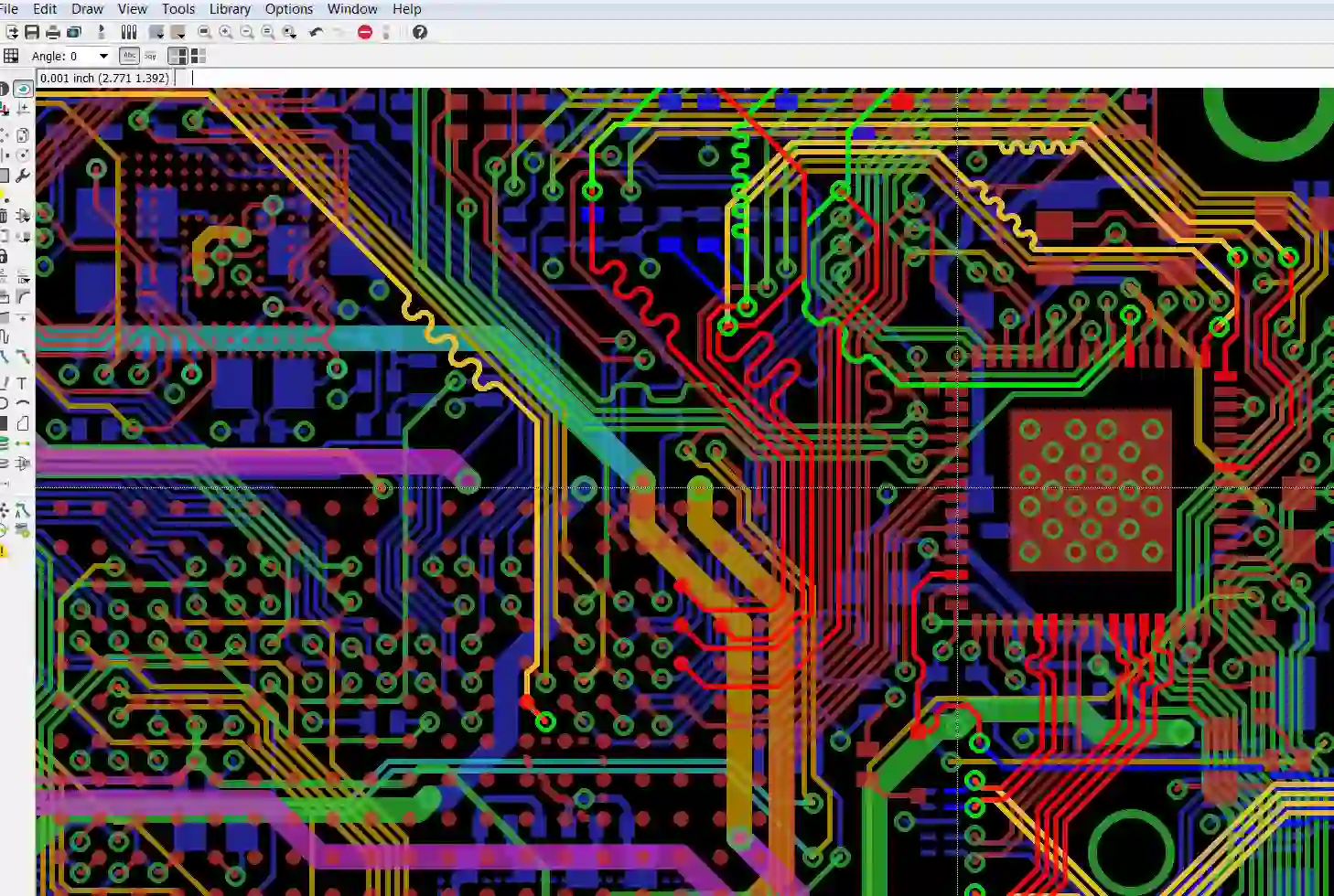
Crosstalk Reduction in Compact Layouts: Managing Interference
Crosstalk happens when signals on adjacent traces interfere with each other, creating noise that can corrupt data in high-speed circuits. In compact PCB layouts, where components and traces are packed closely together, crosstalk is a major concern. The risk increases as trace spacing decreases, especially at frequencies above 1 GHz, where electromagnetic coupling becomes more pronounced.
One effective strategy for crosstalk reduction in compact layouts is to maintain a minimum spacing between traces. A common guideline is the “3W rule,” which suggests that the spacing between adjacent traces should be at least three times the width of the trace to minimize coupling. For instance, if a trace is 5 mils wide, the spacing should be at least 15 mils. Additionally, routing high-speed signals on different layers or using ground planes as shields can further reduce interference.
Another approach is to prioritize differential signaling for critical high-speed lines. Differential pairs, when routed closely together, cancel out external noise and are less susceptible to crosstalk. By optimizing trace spacing and layer stack-up in compact designs, engineers can significantly improve signal quality.
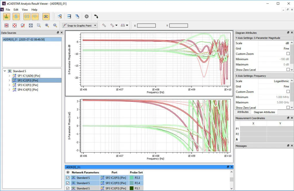
Signal Integrity Simulation for Custom PCB Sizes: A Proactive Approach
Designing PCBs for high-speed digital circuits often involves custom sizes tailored to specific applications, such as wearable devices or industrial modules. However, custom PCB sizes can introduce unique signal integrity challenges that are hard to predict without proper tools. This is where signal integrity simulation becomes invaluable.
Simulation software allows engineers to model how signals behave on a PCB of any size, taking into account factors like trace length, impedance, and crosstalk. For example, a simulation might reveal that a custom small PCB with a 2-inch (50.8 mm) trace length at 2.5 GHz experiences a reflection loss of -20 dB due to an impedance mismatch. Armed with this data, designers can adjust trace routing or add termination components before manufacturing.
Simulation also helps in testing “what-if” scenarios, such as changing the PCB size or material. By running these simulations early, engineers can save time and cost by avoiding multiple prototyping rounds. For custom PCB sizes, integrating signal integrity simulation into the design workflow is a must for ensuring reliable performance.
PCB Material Selection for High-Speed Miniaturization: Choosing Wisely
As devices become smaller, high-speed miniaturization pushes the limits of PCB design. The choice of PCB material is a critical factor in maintaining signal integrity, especially in compact boards where every detail counts. Standard materials like FR-4 are affordable and widely used, but they may not be suitable for high-speed applications above 5 GHz due to their higher dielectric loss and less consistent dielectric constant (typically around 4.2 to 4.5).
For high-speed miniaturization, advanced materials with lower dielectric constants (Dk) and loss tangents (Df) are often preferred. Materials like Rogers RO4350B, with a Dk of 3.48 and Df of 0.0037, offer better signal transmission at high frequencies, reducing loss and maintaining impedance stability in small PCBs. However, these materials come at a higher cost, so engineers must weigh performance needs against budget constraints.
Another consideration is the material’s thermal and mechanical properties, as smaller PCBs in high-speed applications often face heat dissipation challenges. Selecting a material that balances electrical performance with thermal stability ensures long-term reliability in miniaturized designs.
Practical Tips for Optimizing PCB Size in High-Speed Designs
Balancing PCB size with signal integrity in high-speed digital circuits requires a combination of careful planning and advanced techniques. Here are some actionable tips to guide your design process:
- Plan Trace Lengths Early: Calculate critical trace lengths based on signal frequency to avoid reflection and delay issues. Keep traces as short as possible in small PCBs without sacrificing impedance control.
- Use Layer Stack-Ups Effectively: In compact layouts, utilize multiple layers to separate high-speed signals from power and ground planes, reducing crosstalk and EMI.
- Prioritize Ground Planes: A solid ground plane beneath high-speed traces helps maintain consistent impedance and shields against interference, even in smaller boards.
- Test with Simulations: Always simulate signal behavior for custom PCB sizes to identify potential issues before fabrication. Adjust designs based on simulation data for optimal results.
- Select Materials Carefully: Choose PCB materials that support high-speed signals, especially in miniaturized designs where losses are more noticeable.
By following these strategies, you can mitigate the challenges posed by PCB size and ensure robust signal integrity in your high-speed digital circuits.
Conclusion: Striking the Right Balance
The size of a PCB has a profound impact on signal integrity in high-speed digital circuits. Smaller boards, while necessary for compact devices, introduce risks like signal reflection, impedance mismatches, and crosstalk due to tight spacing and limited design flexibility. Larger boards, while offering more room for optimization, can lead to longer traces and increased delays. By focusing on key areas such as PCB size and signal reflection, impedance control in small PCBs, crosstalk reduction in compact layouts, signal integrity simulation for custom PCB sizes, and PCB material selection for high-speed miniaturization, engineers can overcome these challenges.
At ALLPCB, we understand the complexities of high-speed PCB design and are committed to supporting engineers with advanced manufacturing solutions and expertise. Whether you’re working on a miniaturized wearable or a large-scale industrial system, optimizing PCB size for signal integrity is within reach with the right approach and tools. Start planning your next project with these insights in mind, and achieve the performance your designs deserve.