 ALLPCB


In the intricate world of printed circuit board (PCB) manufacturing, achieving precision in quality control is vital. One of the most effective methods to ensure this precision is through PCB microsectioning. But what exactly is microsectioning, and how can it be mastered to analyze PCBs with accuracy? Microsectioning is a process that involves cutting, polishing, and examining a small cross-section of a PCB to reveal its internal structure. This technique is essential for detecting defects, verifying manufacturing quality, and ensuring reliability in electronic devices. In this comprehensive guide, we’ll explore the art of microsectioning, diving deep into PCB microsectioning polishing techniques, the microsectioning etching process, and the best practices for microsectioning PCBs. Whether you’re an engineer, a quality control specialist, or a manufacturer, this blog will provide actionable insights to enhance your PCB analysis.
What is PCB Microsectioning and Why Does It Matter?
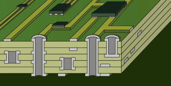
PCB microsectioning, often referred to as cross-sectioning, is a destructive testing method used to inspect the internal layers of a printed circuit board. By cutting a small section of the PCB, preparing it through grinding and polishing, and sometimes etching it, engineers can examine critical features like copper plating thickness, solder joint integrity, and interlayer alignment under a microscope. This process is crucial for identifying issues such as voids, cracks, delamination, or improper plating that could lead to board failure.
The importance of microsectioning cannot be overstated. In industries like aerospace, automotive, and medical devices, where reliability is non-negotiable, a single defect in a PCB can result in catastrophic failures. For instance, a poorly plated through-hole could cause an impedance mismatch, leading to signal loss or delays—potentially critical in high-speed circuits operating at frequencies above 1 GHz. By mastering microsectioning, manufacturers can ensure their boards meet stringent standards and perform reliably in real-world applications.
The Step-by-Step Process of PCB Microsectioning
Microsectioning is a meticulous process that requires precision at every stage. Below, we break down the key steps involved in preparing and analyzing a PCB sample, ensuring you achieve accurate results.
1. Sample Selection and Cutting
The first step in microsectioning is selecting the right area of the PCB for analysis. This could be a region suspected of defects or a representative section of the board. Once selected, the sample is cut using a precision saw, often with a diamond blade, to avoid damaging the delicate internal structures. The goal is to create a clean, flat cross-section without introducing stress or cracks. Typically, the sample size is kept small, around 10-15 mm in width, to make handling and mounting easier.
2. Mounting the Sample
After cutting, the sample is mounted in a resin or epoxy material to hold it securely during grinding and polishing. The mounting material must fully encapsulate the sample to prevent movement and ensure even pressure during preparation. A common practice is to use a cold-mounting epoxy that cures at room temperature to avoid thermal stress on the PCB, which could distort layers or cause delamination.
3. Grinding and Polishing: Key PCB Microsectioning Polishing Techniques
Grinding and polishing are critical to achieving a smooth, mirror-like surface for microscopic analysis. This stage directly impacts the clarity of the final image, so precision is essential. Here are some proven PCB microsectioning polishing techniques:
- Start with Coarse Grinding: Begin with a coarse abrasive, such as 120-grit silicon carbide paper, to remove excess material and flatten the surface. Use a consistent, gentle pressure to avoid uneven grinding.
- Progress to Finer Abrasives: Gradually move to finer grits, such as 400, 800, and 1200, to smooth the surface. Each step reduces scratches from the previous grit, preparing the sample for polishing.
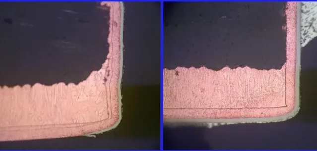
- Final Polishing: Use a polishing cloth with a fine abrasive slurry, often 1-micron or 0.3-micron alumina or diamond paste, to achieve a mirror finish. This step ensures that even the smallest features, like copper plating thicknesses of 25-35 microns, are visible under a microscope.
- Clean Thoroughly: After each grinding and polishing step, clean the sample with isopropyl alcohol or distilled water to remove debris that could cause scratches or obscure details.
4. The Microsectioning Etching Process for Enhanced Visibility
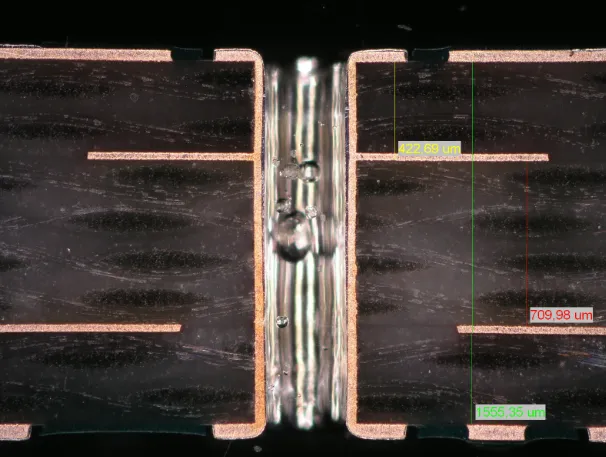
Once the sample is polished, the microsectioning etching process is often applied to reveal specific features of the PCB. Etching uses a chemical solution to selectively remove material or highlight contrasts between different layers, such as copper and dielectric materials. This step is particularly useful for examining grain structures in copper plating or identifying defects like micro-cracks.
A common etchant for copper is a dilute solution of ferric chloride or ammonium persulfate, applied for 10-30 seconds depending on the desired contrast. The process must be carefully controlled to avoid over-etching, which can damage the sample. After etching, rinse the sample immediately with distilled water to stop the reaction, then dry it with compressed air to prevent residue buildup.
For multilayer PCBs, etching can reveal interlayer alignment issues or voids in vias. For example, a poorly filled via might show a void percentage of over 10%, indicating potential reliability issues under thermal cycling conditions (e.g., -40°C to 85°C). Proper etching ensures these defects are visible and measurable during analysis.
5. Microscopic Examination
The final step is to examine the prepared sample under a metallurgical microscope at magnifications ranging from 50x to 1000x. This allows engineers to measure features like copper thickness (typically 1-2 oz, or 35-70 microns), inspect solder joint quality, and identify defects. Digital imaging software can also be used to capture high-resolution images for documentation and further analysis.
Best Practices for Microsectioning PCBs
To achieve consistent, reliable results, following the best practices for microsectioning PCBs is essential. These practices minimize errors, reduce sample damage, and ensure accurate analysis. Here are some key guidelines:
- Use High-Quality Equipment: Invest in precision cutting tools, grinding machines, and microscopes to avoid introducing artifacts or damage during preparation. For instance, a diamond blade with a kerf width of 0.1 mm can minimize material loss during cutting.
- Control Environmental Factors: Perform microsectioning in a clean, temperature-controlled environment to prevent contamination or thermal stress. Maintain a lab temperature of 20-25°C to avoid epoxy curing issues.
- Standardize Procedures: Develop a repeatable process for cutting, grinding, polishing, and etching. Document each step, including abrasive grits used (e.g., 120 to 1200 grit progression) and etching times (e.g., 15 seconds in ferric chloride), to ensure consistency across samples.
- Train Personnel: Ensure that technicians are trained in handling delicate PCB samples and using microsectioning equipment. Mishandling can lead to scratches or cracks, rendering the sample unusable.
- Validate Results: Cross-check measurements with industry standards, such as IPC-6012 for PCB qualification. For example, copper plating in through-holes should meet a minimum thickness of 25 microns to ensure reliability under high-current conditions (e.g., 2-3 A per via).
By adhering to these best practices, you can achieve high-quality microsections that provide valuable insights into PCB performance and manufacturing quality.
Common Challenges in PCB Microsectioning and How to Overcome Them
Despite careful preparation, microsectioning can present challenges that affect the accuracy of analysis. Here are some common issues and solutions:
- Sample Damage During Cutting: Excessive vibration or heat during cutting can cause delamination. Use a low-speed precision saw with adequate coolant to minimize stress.
- Uneven Polishing: Inconsistent pressure during polishing can create an uneven surface, obscuring details. Use automated polishing equipment with adjustable pressure settings (e.g., 10-20 N) for uniform results.
- Over-Etching: Applying etchant for too long can erode critical features. Monitor etching time closely and test on a scrap sample first to determine the optimal duration, usually 10-20 seconds for copper layers.
- Contamination: Dust or debris on the sample can cause scratches or false defects. Clean the sample and workspace regularly, and use filtered air for drying.
Addressing these challenges ensures that your microsectioning process remains accurate and reliable, providing clear visibility into PCB quality.
Applications of Microsectioning in PCB Quality Control
Microsectioning plays a pivotal role in various aspects of PCB quality control and failure analysis. Here are some key applications:
- Plating Quality Assessment: Measures the thickness and uniformity of copper plating in through-holes and vias. For high-reliability boards, plating thickness should be consistent within ±10% of the target (e.g., 30 microns).
- Solder Joint Inspection: Evaluates the integrity of solder joints in surface-mount and through-hole components. Poor wetting or voids over 5% of the joint area can indicate potential failure points.
- Failure Analysis: Identifies root causes of board failures, such as cracks or delamination, after environmental testing (e.g., thermal cycling from -55°C to 125°C).
- Process Validation: Confirms that manufacturing processes meet design specifications, ensuring consistent quality in mass production.
These applications highlight the versatility of microsectioning as a tool for ensuring PCB reliability across industries.
Conclusion: Mastering the Art of Microsectioning for Superior PCB Analysis
The art of microsectioning lies in the delicate balance of precision, technique, and attention to detail. By mastering PCB microsectioning polishing techniques, understanding the microsectioning etching process, and following the best practices for microsectioning PCBs, manufacturers and engineers can gain unparalleled insights into the quality and reliability of their printed circuit boards. From cutting and polishing to etching and microscopic analysis, each step plays a crucial role in revealing the internal structure of a PCB and identifying potential issues before they become costly failures.
Whether you’re working on high-speed circuits with tight impedance tolerances (e.g., 50 ohms ±5%) or producing boards for critical applications, microsectioning is an indispensable tool in your quality control arsenal. With the right techniques and practices, you can ensure that every PCB meets the highest standards of performance and durability. Start refining your microsectioning process today, and take your PCB analysis to the next level.


