 ALLPCB


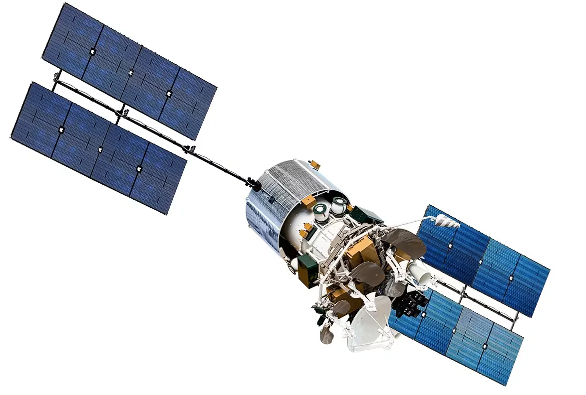
In the unforgiving realm of space exploration, every component of a space probe must perform flawlessly under extreme conditions. Printed Circuit Boards (PCBs) are the backbone of these missions, controlling critical systems like communication, navigation, and data collection. So, how do we ensure space probe PCB reliability to guarantee mission success? At ALLPCB, we understand that high-reliability PCB design for space probes, rigorous testing, and adherence to space-qualified standards are key to overcoming the challenges of harsh space environments. In this blog, we’ll dive deep into the essentials of designing, testing, and analyzing PCBs for space missions, offering practical insights for engineers and mission planners.
Why PCB Reliability is Critical for Space Probes
Space probes operate in environments far beyond the reach of repair teams. A single PCB failure can jeopardize an entire mission, costing millions of dollars and years of research. The stakes are high, as these boards must withstand extreme temperatures ranging from -150°C to 125°C, intense radiation levels up to 100 krad (Si), and vacuum conditions that can cause outgassing of materials. High-reliability PCB design for space probes focuses on durability and fault tolerance to ensure uninterrupted operation over missions that can last decades.
Beyond the physical challenges, PCBs in space probes handle critical tasks like signal processing at speeds exceeding 1 GHz for high-speed data transmission and power management under strict efficiency constraints. A failure in these systems could mean loss of contact with Earth or failure to collect vital scientific data. Let’s explore how to design and test PCBs to meet these demanding requirements.

Key Elements of High-Reliability PCB Design for Space Probes
Designing PCBs for space probes requires a meticulous approach to material selection, layout, and manufacturing. Here are the core principles that ensure reliability in the harshest of environments.
1. Material Selection for Extreme Conditions
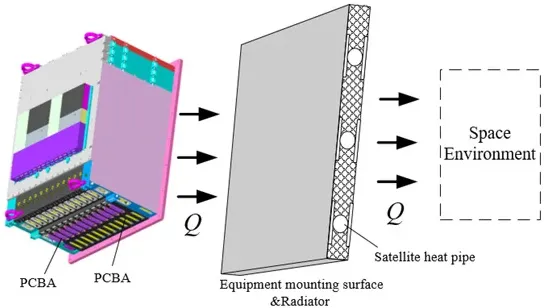
Standard PCB materials like FR-4 are unsuitable for space applications due to their poor performance under temperature extremes and radiation. Instead, high-reliability designs often use polyimide or ceramic substrates, which offer thermal stability from -200°C to 300°C and resist radiation-induced degradation. These materials also have low outgassing properties, critical in a vacuum to prevent contamination of sensitive instruments.
Copper traces and vias must be designed with high purity and thickness (typically 2 oz or 70 μm) to handle high currents without overheating. Additionally, conformal coatings or encapsulation with materials like silicone or epoxy protect against moisture and radiation, extending the PCB’s lifespan.
2. Layout Optimization for Signal Integrity
Space probe PCBs often manage high-frequency signals for communication systems, requiring impedance control within ±10% of the target value (e.g., 50 ohms for RF lines). Poor impedance matching can lead to signal reflection and data loss, critical issues when transmitting information across millions of kilometers. Designers use controlled dielectric constants (typically 3.5 to 4.5) and minimize trace lengths to reduce latency and crosstalk.
Power distribution networks (PDNs) must also be optimized to handle voltage drops under 2% to prevent system instability. Decoupling capacitors placed close to ICs help maintain stable power delivery, even under fluctuating loads during mission phases like launch or planetary entry.
3. Redundancy and Fault Tolerance
In space, there’s no room for single-point failures. High-reliability PCB design incorporates redundancy by duplicating critical circuits and using fault-tolerant architectures. For instance, dual power supplies with automatic failover mechanisms ensure continuous operation if one system fails. Designers also use error-correcting code (ECC) memory to mitigate radiation-induced bit flips, a common issue in space environments.
Space Probe PCB Failure Analysis: Identifying and Preventing Issues
Understanding why PCBs fail in space missions is as important as designing them for reliability. Space probe PCB failure analysis helps engineers identify weak points and improve future designs. Common failure modes include thermal fatigue, radiation damage, and mechanical stress from launch vibrations.
1. Thermal Fatigue and Material Stress
Space probes experience rapid temperature swings, causing expansion and contraction of PCB materials. Over time, this thermal cycling can lead to cracks in solder joints or delamination of layers. Failure analysis often reveals that joints subjected to over 1000 thermal cycles (from -55°C to 125°C) show a 20% higher failure rate if not designed with flexible materials or stress-relief techniques.
2. Radiation-Induced Failures
Radiation in space can cause single-event upsets (SEUs) or total ionizing dose (TID) effects, degrading semiconductor components on the PCB. Analysis of failed boards often shows cumulative doses above 50 krad (Si) leading to threshold voltage shifts in transistors. Shielding with materials like tantalum (1 mm thick) or using radiation-hardened components can reduce these risks by up to 40%.
3. Mechanical Failures from Vibration
During launch, space probes endure vibrations with frequencies up to 2000 Hz and accelerations of 10g or more. These forces can cause micro-cracks in traces or component detachment. Post-mission analysis often uses X-ray imaging to detect hidden fractures, informing better mounting techniques or damping solutions for future designs.
PCB Testing for Space Missions: Rigorous Standards for Reliability
Testing is the cornerstone of ensuring that PCBs can survive the rigors of space. PCB testing for space missions follows strict protocols to simulate the extreme conditions of launch and operation. Here’s how testing ensures mission readiness.
1. Environmental Testing
PCBs undergo thermal cycling tests between -65°C and 150°C for hundreds of cycles to mimic space temperature swings. Vacuum testing ensures no outgassing occurs, as even 0.1% material loss can contaminate onboard optics. Radiation testing exposes boards to doses up to 100 krad (Si) to verify component stability, often using cobalt-60 sources to simulate space radiation.
2. Vibration and Shock Testing
To replicate launch conditions, PCBs are subjected to random vibration tests at 20-2000 Hz and shock tests with peak accelerations of 3000g. These tests confirm that components remain securely attached and traces don’t fracture under stress. A pass rate of 99% or higher is typically required before a board is mission-ready.
3. Electrical Performance Testing
Signal integrity tests measure parameters like insertion loss (under 3 dB at 1 GHz) and crosstalk (below -30 dB) to ensure reliable data transmission. Power integrity tests verify that voltage ripple stays under 50 mV during load changes, critical for stable operation of onboard systems.
Space-Qualified PCB Standards: Meeting Industry Benchmarks
Adhering to space-qualified PCB standards ensures that designs meet the stringent requirements of space agencies and mission planners. These standards provide a framework for reliability and performance in extreme environments.
1. ECSS Standards for European Missions
The European Cooperation for Space Standardization (ECSS) outlines guidelines like ECSS-Q-ST-70-12C for PCB design and manufacturing. These standards mandate the use of high-reliability materials, prohibit certain solders prone to whiskering (like pure tin), and require 100% inspection of solder joints for defects.
2. NASA and MIL-SPEC Standards
NASA’s standards, such as those from the NASA Electronic Parts and Packaging (NEPP) program, emphasize radiation hardness and thermal performance. MIL-PRF-31032, a military specification often adopted for space, requires PCBs to pass environmental stress screening (ESS) with zero failures before deployment.
3. IPC Class 3 for Aerospace
IPC Class 3 standards, the highest reliability class, are often used for space PCBs. They demand tight tolerances (e.g., trace width variation under ±10%) and rigorous testing to ensure boards can operate without failure in life-critical applications.
Practical Tips for Engineers Designing Space Probe PCBs
For engineers tasked with creating reliable PCBs for space probes, here are actionable tips to enhance design and testing processes:
- Simulate Early and Often: Use simulation tools to model thermal and radiation effects before prototyping. This can reduce design iterations by up to 30%.
- Partner with Experts: Work with manufacturing teams familiar with space-qualified standards to avoid costly errors during production.
- Prioritize Documentation: Maintain detailed records of every design and test phase to streamline failure analysis if issues arise post-launch.
- Test Beyond Requirements: Exceed minimum testing thresholds by 10-20% to build a safety margin into your designs.
Conclusion: Building the Future of Space Exploration with Reliable PCBs
The success of space probes hinges on the reliability of their smallest components, especially PCBs. By focusing on high-reliability PCB design for space probes, conducting thorough space probe PCB failure analysis, implementing rigorous PCB testing for space missions, and adhering to space-qualified PCB standards, engineers can ensure that these critical systems withstand the harsh conditions of space. At ALLPCB, we’re committed to supporting the space industry with expertise and solutions tailored for mission-critical applications. Together, we can push the boundaries of exploration, one reliable PCB at a time.


