 ALLPCB


Designing a printed circuit board (PCB) involves much more than just placing components and routing traces. One of the most critical aspects is defining the PCB outline, which sets the physical boundaries of the board and ensures it fits into its intended application while meeting manufacturing constraints. So, what are the key PCB outline design rules to follow for manufacturability and compatibility? In short, you must focus on proper clearance, spacing, edge definition, and alignment with manufacturing capabilities to avoid costly errors and delays.
In this comprehensive guide, we’ll dive deep into the specifics of PCB outline design rules, covering essential topics like PCB outline clearance, PCB outline spacing, and PCB outline edge definition. Whether you're a beginner or an experienced designer, this blog will provide actionable insights to help you create boards that are both functional and easy to manufacture.
Why PCB Outline Design Rules Matter
The PCB outline is the physical shape and boundary of your board. It determines how the board fits into an enclosure, interacts with other components, and aligns with the manufacturing process. Ignoring PCB outline design rules can lead to issues such as boards that don’t fit into their housing, components too close to edges causing assembly problems, or even manufacturing defects due to improper spacing or clearance.
Following these rules ensures that your design is compatible with standard manufacturing processes, reduces the risk of errors, and saves time and money. Let’s break down the key elements of PCB outline design to help you achieve a successful build.
Understanding PCB Outline Design Basics
Before diving into specific rules, it’s important to understand what a PCB outline represents. The outline defines the exact shape and dimensions of the board, including any cutouts, notches, or mounting holes. It’s typically drawn in your PCB design software on a dedicated layer, often called the "board outline" or "mechanical layer."
A well-defined outline ensures that the board can be cut accurately during fabrication and fits perfectly into its intended application. Now, let’s explore the specific rules and guidelines that govern PCB outline design for manufacturability and compatibility.
1. PCB Outline Clearance: Keeping Components Safe
PCB outline clearance refers to the minimum distance between the edge of the board and any components, traces, or vias. This clearance is crucial to prevent damage during manufacturing processes like depanelization (separating individual boards from a larger panel) and to ensure that components aren’t too close to the edge where they could be affected by mechanical stress or environmental factors.
As a general rule, maintain a clearance of at least 0.5 mm (20 mils) between the board edge and any components or traces. However, this value can vary based on the manufacturer’s capabilities and the complexity of your design. For high-density designs, you might need to consult with your fabrication house to confirm their minimum clearance requirements.
For example, if you’re designing a board for a compact device, placing components too close to the edge might result in them being damaged during cutting or handling. A safe clearance also allows room for edge connectors or mounting hardware without risking interference.
2. PCB Outline Spacing: Avoiding Manufacturing Conflicts
PCB outline spacing is closely related to clearance but focuses more on the spacing between the board outline and other design elements like cutouts, slots, or adjacent boards in a panelized design. Proper spacing ensures that the cutting tools used in manufacturing can operate without damaging nearby features.
A common guideline for PCB outline spacing is to maintain at least 1.6 mm (63 mils) between the edges of adjacent boards in a panel or between the outline and internal cutouts. This spacing accounts for the width of the cutting tool (often a router bit) and prevents stress fractures or jagged edges during depanelization.
For instance, if your design includes multiple small boards on a single panel, insufficient spacing could lead to inaccurate cuts or even damage to the boards. Always check with your manufacturer for their specific spacing requirements, as some may use different tools or processes that affect the minimum distance.
3. PCB Outline Edge Definition: Precision in Shape and Corners
PCB outline edge definition refers to how precisely the edges and corners of the board are defined in your design. This includes specifying whether corners are sharp or rounded, as well as the radius of any rounded corners. Clear edge definition is essential for ensuring that the board matches its intended shape and fits into its enclosure or assembly.
Most manufacturers prefer rounded corners over sharp ones because sharp corners can create stress points that lead to cracking during manufacturing or handling. A typical corner radius is 0.5 mm to 1.0 mm, but this can vary based on the board’s size and application. Additionally, internal cutouts or slots should also have rounded edges to avoid similar issues.
For example, if your PCB is designed to fit into a tight enclosure, a poorly defined edge or an overly sharp corner might prevent a proper fit or cause mechanical stress. Clearly defining the edge in your design files and adhering to the manufacturer’s guidelines can prevent these problems.
4. Material and Thickness Considerations for the Outline
The material and thickness of your PCB also play a role in outline design. Standard PCB materials like FR-4 have specific mechanical properties that affect how the board can be cut and shaped. Thicker boards (e.g., 2.0 mm or more) may require larger spacing or clearance due to the increased difficulty in cutting, while thinner boards (e.g., 0.8 mm) might be more prone to warping if the outline isn’t carefully designed.
For instance, a 1.6 mm thick FR-4 board is a common choice for many applications and typically works well with standard outline design rules. However, if you’re using a thinner board for a flexible or lightweight design, you might need to increase clearance to prevent damage during handling.
Always specify the material and thickness in your design documentation, and confirm with your manufacturer if there are any limitations or special requirements for the outline based on your chosen specifications.
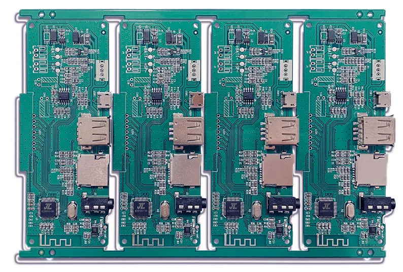
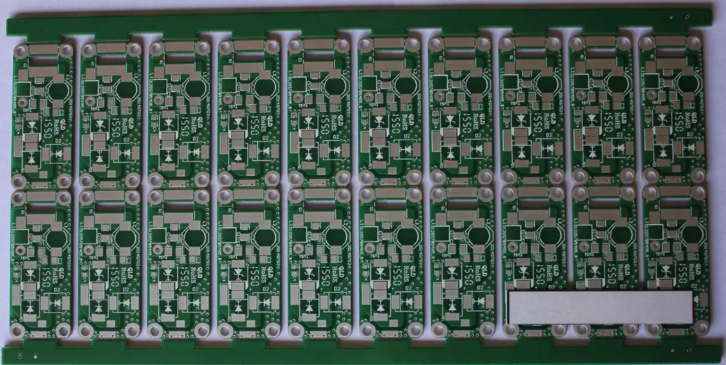
5. Panelization and Breakaway Tabs for Efficient Manufacturing
Panelization is the process of grouping multiple PCBs onto a single panel for manufacturing. Proper PCB outline design rules must account for how the boards will be separated after fabrication. Breakaway tabs (also called mouse bites) are small perforated connections that hold the boards together in the panel but allow them to be easily separated by hand or machine.
When designing breakaway tabs, ensure they are placed in areas that won’t interfere with components or critical traces. A typical tab width is 2.0 mm to 3.0 mm, with small holes (around 0.8 mm in diameter) spaced evenly along the tab to create the perforation. Leave at least 2.5 mm of clearance between the tab and any components to avoid damage during separation.
PCB panelization not only improves manufacturing efficiency but also reduces costs by maximizing the number of boards produced per panel. However, improper tab placement or spacing can lead to uneven breaks or damage to the board edges.
Best Practices for PCB Outline Design Compatibility
Beyond the specific rules for clearance, spacing, and edge definition, there are several best practices to ensure your PCB outline design is compatible with both manufacturing processes and the end application.
- Consult Manufacturer Guidelines Early: Every fabrication house has slightly different capabilities and requirements. Before finalizing your outline, review their design guidelines or speak with their support team to confirm details like minimum clearance or preferred corner radius.
- Use Standard Shapes When Possible: Complex or irregular shapes can increase manufacturing costs and lead to errors. Stick to standard rectangular or square outlines unless your application specifically requires a unique shape.
- Include Mounting Holes in the Outline: If your board needs mounting holes for assembly, include them in the outline design with proper clearance from the edge (typically 3.0 mm or more). Specify the hole size and tolerance to ensure compatibility with screws or fasteners.
- Test Fitment with 3D Models: If your PCB must fit into an enclosure, use 3D modeling tools in your design software to simulate the fit. This can help identify potential issues with the outline before manufacturing.
Common Mistakes to Avoid in PCB Outline Design
Even experienced designers can make mistakes when defining a PCB outline. Here are some common pitfalls to watch out for:
- Ignoring Clearance Near Edges: Placing components or traces too close to the board edge can lead to damage during cutting or handling. Always adhere to minimum clearance rules.
- Overlooking Internal Cutouts: Internal slots or cutouts need the same attention to spacing and edge definition as the outer outline. Failing to account for tool limitations can result in inaccurate cuts.
- Not Specifying Layer Information: Ensure the outline is clearly marked on the correct layer in your design files. Miscommunication here can lead to manufacturing errors.
- Forgetting Panelization Needs: If you’re producing multiple boards, failing to design for panelization can increase costs or cause delays. Plan for spacing and breakaway tabs from the start.
How to Verify Your PCB Outline Design
Before sending your design for fabrication, take the time to verify the PCB outline. Most design software includes tools like Design Rule Checks (DRC) that can automatically flag issues with clearance, spacing, or edge definition. Run these checks to catch potential errors early.
Additionally, export your outline layer as a separate file or include clear documentation in your manufacturing package. This helps the fabrication team understand your intent and reduces the risk of misinterpretation.
Finally, consider requesting a prototype run for complex designs. Testing a physical sample can reveal fitment or manufacturing issues that might not be apparent in digital simulations.
Conclusion: Mastering PCB Outline Design Rules
Designing a PCB outline that ensures manufacturability and compatibility requires attention to detail and adherence to key rules like PCB outline clearance, PCB outline spacing, and PCB outline edge definition. By maintaining proper distances, defining edges clearly, and following manufacturer guidelines, you can avoid common pitfalls and create boards that are both functional and cost-effective to produce.
Remember to plan for panelization, account for material properties, and verify your design before fabrication. With these practices in place, you’ll be well on your way to creating high-quality PCBs that meet the needs of your application. Keep these guidelines handy for your next project, and you’ll save time, reduce errors, and achieve better results.


