 ALLPCB


In the world of electronics manufacturing, ensuring the safe delivery of printed circuit boards (PCBs) is critical. How can you minimize damage during PCB logistics? The answer lies in adopting proper handling techniques, including ESD-safe transport, moisture control, and shock-resistant packaging. In this comprehensive guide, we’ll dive deep into PCB handling best practices to help you protect your valuable components during transportation and storage. Whether you're an engineer, manufacturer, or logistics professional, these actionable tips will ensure your PCBs arrive in perfect condition, ready for assembly or installation.
Why Proper PCB Handling Matters in Logistics
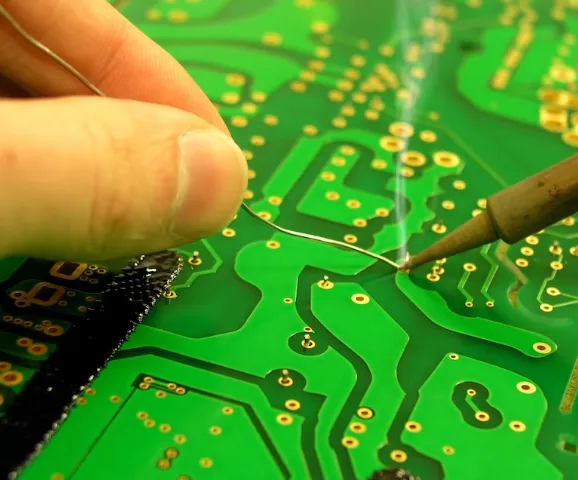
PCBs are the backbone of modern electronics, powering everything from smartphones to industrial machinery. However, these delicate components are highly susceptible to damage from electrostatic discharge (ESD), moisture, physical shock, and environmental hazards. A single mishandling incident can lead to costly failures, delayed production, or compromised product reliability. According to industry studies, nearly 30% of electronic failures are attributed to improper handling or storage during logistics. By implementing best practices for PCB handling, you can significantly reduce these risks and maintain the integrity of your products.
Understanding the Risks in PCB Logistics
Before diving into solutions, it’s important to understand the primary risks that PCBs face during transportation and storage. These risks include:
- Electrostatic Discharge (ESD): A sudden flow of electricity between two objects can damage sensitive components on a PCB, leading to immediate failure or latent defects.
- Moisture Exposure: Humidity can cause corrosion, delamination, or popcorn effects during soldering due to absorbed moisture in PCB materials.
- Physical Shock and Vibration: Drops, impacts, or excessive vibration during transit can crack solder joints, dislodge components, or damage the board itself.
- Temperature Extremes: High or low temperatures can warp PCBs or affect the performance of onboard components.
Addressing these risks with proper handling techniques ensures that your PCBs remain functional and reliable, no matter the distance they travel.
PCB Handling Best Practices for Safe Logistics
Let’s explore the core strategies for minimizing damage during PCB logistics. These best practices focus on protecting boards from ESD, moisture, shock, and other environmental factors.
1. ESD-Safe PCB Transport: Protecting Against Static Damage
Electrostatic discharge is one of the most common causes of PCB damage. A discharge as small as 100 volts can harm sensitive components, even if the damage isn’t immediately visible. To ensure ESD-safe PCB transport, follow these guidelines:
- Use ESD-Safe Packaging: Always store and transport PCBs in anti-static bags or containers made from conductive or dissipative materials. These materials prevent static buildup and safely dissipate any charge.
- Ground Handling Personnel: Ensure that anyone handling PCBs wears ESD wrist straps or works on grounded mats to prevent static discharge.
- Avoid High-Static Environments: Keep PCBs away from areas with low humidity or materials like plastic films that generate static electricity.
By prioritizing ESD-safe practices, you can protect your PCBs from unseen but devastating damage. For instance, using an anti-static bag with a surface resistivity of 10^6 to 10^9 ohms per square can effectively shield components during transit.

2. Moisture Control in PCB Logistics: Preventing Corrosion and Defects
Moisture is a silent enemy of PCBs, especially during long-distance shipping or storage in humid environments. Absorbed moisture can lead to issues like corrosion of copper traces or “popcorning” during reflow soldering, where trapped moisture expands and damages the board. Here’s how to ensure moisture control in PCB logistics:
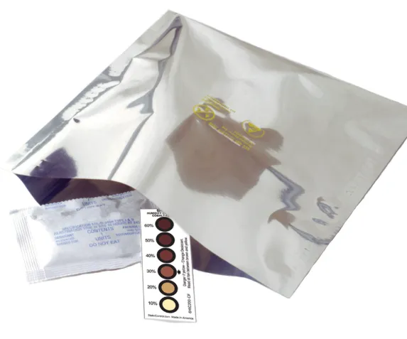
- Use Moisture Barrier Bags (MBBs): Seal PCBs in MBBs with a vapor barrier layer to block humidity. These bags often meet standards like MIL-PRF-81705 for maximum protection.
- Include Desiccants: Place silica gel packets or other desiccants inside the packaging to absorb any residual moisture. A common guideline is to use 1 unit of desiccant per 1.2 cubic feet of enclosed space.
- Add Humidity Indicator Cards (HICs): Include HICs inside the packaging to monitor moisture levels. If the card shows a humidity level above 10%, it’s a sign that the package needs resealing or additional desiccants.
- Store in Controlled Environments: When possible, store PCBs in areas with relative humidity below 50% and temperatures between 18-22°C (64-72°F).
Implementing these moisture control measures can prevent long-term damage and ensure your PCBs are ready for assembly upon arrival.
3. Shock-Resistant Packaging for PCBs: Cushioning Against Impact
Physical damage from shocks or vibrations during transit can render a PCB unusable. A drop from just a few feet can crack the board or loosen components, leading to costly rework. To minimize these risks, invest in shock-resistant packaging for PCBs with these techniques:
- Use Foam Inserts or Cushioning: Place PCBs in custom-cut foam inserts or bubble wrap to absorb shocks. Ensure the foam has a density of at least 1.8 pounds per cubic foot for adequate protection.
- Secure Boards in Rigid Containers: Use sturdy boxes or containers made from corrugated cardboard or plastic with a minimum burst strength of 200 pounds per square inch to withstand external pressure.
- Avoid Overpacking: Don’t stack too many PCBs in a single container, as this can lead to crushing or excessive pressure on the bottom boards. A general rule is to leave at least 1 inch of space between stacked PCBs with protective layers in between.
- Label Packages as Fragile: Clearly mark shipping boxes with “Fragile” or “Handle with Care” labels to alert handlers to the delicate contents.
Shock-resistant packaging is especially crucial for international shipments, where packages may endure rough handling or long journeys. By cushioning your PCBs properly, you can avoid mechanical failures and maintain product quality.
4. Temperature Management: Avoiding Thermal Stress
Extreme temperatures during logistics can warp PCBs or degrade component performance. For example, prolonged exposure to temperatures above 85°C (185°F) can cause delamination in multilayer boards, while freezing temperatures below 0°C (32°F) can make materials brittle. Follow these tips to manage temperature:
- Use Insulated Packaging: For shipments through extreme climates, use insulated boxes or thermal liners to maintain a stable internal temperature.
- Monitor Temperature During Transit: Attach temperature data loggers to critical shipments to track exposure. Aim to keep PCBs within a range of 5-35°C (41-95°F) during transport.
- Avoid Direct Sunlight: Store and transport PCBs away from direct sunlight, which can cause uneven heating and thermal stress.
Temperature management is often overlooked in PCB logistics, but it plays a vital role in preserving board integrity, especially for sensitive or high-value designs.
Additional Tips for Streamlined PCB Logistics
Beyond the core handling techniques, consider these additional strategies to optimize your PCB logistics process:
- Train Staff on Handling Protocols: Ensure all personnel involved in PCB handling are trained on ESD safety, moisture control, and proper packaging methods. Regular training can reduce human error by up to 40%, according to workplace safety studies.
- Partner with Reliable Logistics Providers: Choose shipping partners with experience in handling electronics and a track record of minimal damage claims. Look for providers offering climate-controlled transport options.
- Document and Inspect Shipments: Keep detailed records of packaging methods and inspect incoming PCBs for signs of damage or exposure. This helps identify weak points in your logistics chain for future improvement.
Creating a Comprehensive PCB Handling Checklist
To simplify the process, develop a checklist for PCB logistics that covers all critical aspects of handling and transport. Here’s a sample checklist to get you started:
- Pack PCBs in ESD-safe anti-static bags or containers.
- Seal packages in moisture barrier bags with desiccants and humidity indicators.
- Use shock-resistant packaging with foam inserts or cushioning.
- Label boxes as “Fragile” and include handling instructions.
- Monitor temperature and humidity during storage and transit.
- Train staff on proper handling techniques.
- Inspect shipments upon arrival for damage or exposure.
Using a checklist ensures consistency and minimizes the risk of oversight, especially for large-scale operations.
The Benefits of Proper PCB Handling in Logistics
Investing time and resources into proper PCB handling techniques offers numerous benefits, including:
- Reduced Costs: Fewer damaged boards mean lower replacement and rework expenses.
- Improved Reliability: Protected PCBs perform better and last longer, enhancing overall product quality.
- Faster Production Cycles: Avoiding delays due to damaged shipments keeps your projects on schedule.
- Customer Satisfaction: Delivering flawless PCBs builds trust with clients and strengthens business relationships.
Conclusion: Safeguarding Your PCBs for Success
PCB logistics is a critical yet often overlooked aspect of electronics manufacturing. By adopting PCB handling best practices, such as ESD-safe PCB transport, moisture control in PCB logistics, and shock-resistant packaging for PCBs, you can minimize damage and ensure your boards arrive in pristine condition. From using anti-static bags to implementing temperature monitoring, every step plays a vital role in protecting your investment. Start by reviewing your current handling processes and integrating the tips shared in this guide. With the right approach, you’ll safeguard your PCBs against the challenges of transit and storage, paving the way for successful projects and satisfied customers.


