 ALLPCB


When designing a printed circuit board (PCB) for radio frequency (RF) applications, every detail matters. One often overlooked choice is the solder mask finish—matte or glossy. So, which is better for your RF design? In short, matte solder mask is generally preferred for RF PCBs due to its lower reflectivity and better performance in high-frequency applications, while glossy solder mask may impact signal integrity due to potential interference. However, the decision depends on your specific project needs, such as impedance control and environmental factors. In this blog, we’ll dive deep into the differences between matte solder mask for RF PCB and glossy solder mask for signal integrity, helping you make an informed choice for high-frequency applications.
Understanding Solder Mask and Its Role in RF PCB Design
A solder mask is a thin protective layer applied to the copper traces of a PCB. It prevents oxidation, protects against environmental damage, and stops solder from bridging between components during assembly. In RF PCB design, the solder mask plays an even more critical role. At high frequencies, even small variations in materials or surface finish can affect signal integrity and impedance control.
For high-frequency applications, the solder mask must minimize signal loss and interference. Its dielectric properties, thickness, and finish can influence how signals travel across the board. This is why choosing between a matte or glossy finish isn’t just about looks—it’s about performance. Let’s explore how these finishes differ and what they mean for your RF design.
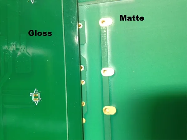
Matte Solder Mask for RF PCB: Benefits and Drawbacks
Matte solder mask has a non-reflective, textured finish. It’s often chosen for RF designs because of its unique properties that support high-frequency performance. Here’s a closer look at why it might be the right choice for your project.
Benefits of Matte Solder Mask in High-Frequency Applications
- Reduced Signal Reflection: The non-shiny surface of matte solder mask minimizes light and electromagnetic reflection. In RF designs, this can help reduce unwanted interference that might degrade signal integrity. Studies suggest that reflective surfaces can contribute to noise in high-frequency circuits, making matte a safer bet.
- Better Adhesion: Matte finishes often provide better adhesion for components and markings. This is crucial in RF PCBs where precise placement and stability are necessary to maintain impedance control.
- Lower Dielectric Impact: While the dielectric constant of solder mask material matters more than the finish, matte finishes are sometimes paired with materials optimized for RF. This can result in less signal loss, especially at frequencies above 1 GHz.
Drawbacks of Matte Solder Mask
- Less Aesthetic Appeal: Matte finishes aren’t as visually striking as glossy ones. If your project requires a polished look for client presentations or marketing, this could be a downside.
- Potential for Dust Accumulation: The textured surface can trap dust or contaminants over time, which might be a concern in harsh environments unless additional protective measures are taken.
For many RF engineers, the performance benefits of matte solder mask outweigh these minor drawbacks. If signal integrity at high frequencies (like 5 GHz or above) is your priority, matte is often the go-to choice.
Glossy Solder Mask and Signal Integrity: Advantages and Challenges
Glossy solder mask has a smooth, shiny finish that reflects light. While it’s popular for its sleek appearance, its impact on RF designs, especially regarding signal integrity, needs careful consideration. Let’s break down its pros and cons for high-frequency applications.
Advantages of Glossy Solder Mask
- Visual Appeal: The shiny finish looks professional and clean, making it a popular choice for consumer electronics or display boards where aesthetics matter.
- Easier Cleaning: Unlike matte finishes, glossy surfaces are less likely to trap dirt or debris, which can be beneficial in environments where cleanliness is a priority.
- Smoother Surface: The smooth texture can reduce friction during assembly processes, potentially lowering the risk of damage to delicate components.
Challenges of Glossy Solder Mask in RF Designs
- Increased Reflectivity: The reflective nature of glossy solder mask can introduce unwanted electromagnetic interference in high-frequency applications. This might lead to signal reflections or crosstalk, especially in designs operating at frequencies above 2.4 GHz, such as Wi-Fi or 5G systems.
- Impact on Signal Integrity: Glossy finishes may contribute to higher parasitic capacitance due to their surface properties. This can alter impedance, which is critical for RF circuits where controlled impedance (often 50 ohms) is necessary for optimal performance.
- Inspection Challenges: The reflective surface can make it harder to spot defects or misalignments during visual inspections, potentially leading to quality issues in production.
While glossy solder mask has its place in low-frequency or non-critical designs, it often falls short in RF applications where signal integrity and impedance control are paramount.
Solder Mask Finish Comparison: Key Factors for RF Design
Choosing between matte and glossy solder mask for your RF PCB design involves evaluating several key factors. Below, we compare these finishes based on criteria essential for high-frequency applications.
1. Signal Integrity and Performance
In RF designs, maintaining signal integrity is non-negotiable. Matte solder mask typically performs better by reducing interference and supporting consistent signal transmission. For instance, in a 5G antenna design operating at 28 GHz, even a 1% signal loss due to reflection can degrade performance. Glossy finishes, with their higher reflectivity, are more likely to introduce such issues.
2. Impedance Control
Impedance control is critical in RF circuits to ensure signals travel without distortion. The solder mask’s dielectric properties and thickness play a role here. While the finish itself (matte or glossy) has a minor direct impact, matte finishes are often paired with RF-optimized materials that maintain a stable dielectric constant (Dk) around 3.5 to 4.0, supporting consistent 50-ohm impedance. Glossy masks, if not carefully selected, might contribute to slight variations in capacitance, affecting impedance.
3. Environmental Durability
RF PCBs are often used in challenging environments, from telecom towers to automotive radar systems. Matte finishes might collect dust, but they offer better adhesion for protective coatings. Glossy finishes resist dirt but may crack or wear under thermal stress, exposing copper traces to corrosion.
4. Manufacturing and Cost Considerations
Both matte and glossy solder masks are widely available and don’t significantly differ in cost. However, matte finishes might require more precise application to avoid uneven textures, while glossy finishes can sometimes mask minor application flaws due to their shine. For high-volume RF production, this could influence your choice based on quality control needs.
How to Choose the Right Solder Mask Finish for Your RF Project
With the differences between matte and glossy solder mask clear, how do you decide which is right for your RF design? Consider the following steps to guide your decision.
Step 1: Define Your Frequency Range
If your project operates at frequencies below 1 GHz, such as in some IoT devices, the finish might not be as critical, and glossy could work if aesthetics are important. However, for applications above 1 GHz—like 5G, radar, or satellite systems—matte solder mask is almost always the safer choice to minimize interference.
Step 2: Assess Impedance Requirements
Check your design’s impedance needs. If tight control (e.g., maintaining 50 ohms with a tolerance of ±5%) is essential, prioritize a solder mask material and finish that supports this. Matte finishes, paired with low-Dk materials, often provide better consistency.
Step 3: Evaluate Environmental Conditions
Will your PCB be exposed to dust, moisture, or extreme temperatures? Matte finishes might need extra protection in dusty environments, while glossy finishes could wear faster under thermal cycling. Choose based on the harshest conditions your board will face.
Step 4: Balance Aesthetics and Functionality
If your PCB will be visible in a final product or demo, a glossy finish might appeal more to stakeholders. However, never compromise signal integrity for looks in critical RF applications. Matte can still look professional with proper design.
Practical Tips for Optimizing Solder Mask in RF Designs
Beyond choosing between matte and glossy, here are some actionable tips to ensure your solder mask supports your RF design goals.
- Minimize Solder Mask Over RF Traces: Where possible, avoid applying solder mask over critical RF transmission lines. Exposed traces with controlled impedance perform better, as solder mask can introduce parasitic capacitance. If protection is needed, use a thin layer and opt for matte to reduce interference.
- Select Low-Dk Materials: Work with solder mask materials designed for RF, with dielectric constants below 4.0. This reduces signal loss regardless of finish.
- Test and Validate: Use simulation tools to model how solder mask finish affects signal integrity in your specific layout. Then, prototype and test with real-world conditions to confirm performance.
- Consult with Your Manufacturer: Different fabrication processes can affect how matte or glossy finishes behave. Collaborate early to ensure the chosen finish aligns with your design specs.
Conclusion: Making the Right Choice for Your RF PCB
Choosing between matte and glossy solder mask for your RF design isn’t just a cosmetic decision—it directly impacts signal integrity, impedance control, and overall performance in high-frequency applications. Matte solder mask often stands out as the better choice for RF PCBs due to its ability to minimize reflections and support consistent signal transmission, especially at frequencies above 1 GHz. Glossy solder mask, while visually appealing, can introduce challenges like increased interference and potential impedance variations.
At ALLPCB, we understand the nuances of RF design and are here to support you in selecting the optimal solder mask finish for your project. By considering your frequency range, impedance needs, and environmental factors, you can make a decision that ensures both functionality and reliability. Whether you’re designing for 5G, radar, or IoT, the right solder mask finish can make all the difference in achieving top-tier performance.


