ALLPCB


In the fast-evolving world of technology, the Internet of Things (IoT) is transforming how we monitor and manage systems remotely. One key challenge for IoT devices, especially remote sensors and wireless devices, is ensuring a reliable power source in off-grid or hard-to-reach locations. This is where solar PCBs (Printed Circuit Boards) come into play. Designed to harness solar energy, solar PCBs provide a sustainable and efficient power solution for IoT applications. In this blog, we’ll explore how solar PCBs are used in IoT, focusing on applications like remote monitoring and wireless sensors, and dive into design considerations such as low power and energy harvesting.
What Are Solar PCBs and Why Are They Vital for IoT?
Solar PCBs are specialized circuit boards integrated with components to capture, store, and manage solar energy. They are often paired with photovoltaic cells to convert sunlight into electricity, powering devices without reliance on traditional power grids. For IoT systems, which often include sensors and wireless devices deployed in remote areas, solar PCBs offer a game-changing solution. They eliminate the need for frequent battery replacements and reduce maintenance costs, making them ideal for long-term, sustainable operations.
IoT applications such as environmental monitoring, smart agriculture, and industrial automation benefit greatly from solar PCB for IoT sensors. These boards ensure continuous operation in locations where wiring or battery swaps are impractical. Let’s dive deeper into the specific applications and design approaches that make solar PCBs a cornerstone of modern IoT solutions.
Key IoT Applications of Solar PCBs
1. Remote Monitoring with Solar PCBs
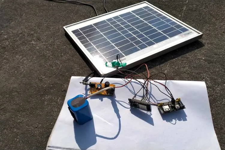
Remote monitoring systems are a prime application for remote monitoring solar PCB designs. These systems are used in industries like environmental science, infrastructure management, and disaster prevention to track conditions in real-time. For instance, weather stations in remote forests or deserts use solar-powered IoT sensors to measure temperature, humidity, and wind speed, transmitting data via wireless networks.
A typical setup might include a solar PCB with a small photovoltaic panel generating 5-10 watts of power under direct sunlight. This energy charges a lithium-ion battery with a capacity of around 3.7V and 2000mAh, ensuring the sensor operates even during cloudy conditions or at night. The PCB manages power distribution, ensuring the sensor and wireless module (often operating at 3.3V) receive stable voltage with minimal loss—typically achieving an efficiency of 85-90% in modern designs.
By using solar PCBs, these systems can operate for years without human intervention, reducing operational costs by up to 60% compared to battery-only solutions. This makes them indispensable for tracking remote assets or environmental changes in areas with no access to electricity.
2. Solar-Powered Wireless Sensor Networks
Wireless sensor networks (WSNs) are widely used in smart agriculture, industrial monitoring, and security systems. A solar powered wireless sensor PCB enables these networks to function independently by providing a consistent power source. For example, in precision farming, sensors monitor soil moisture and temperature, sending data to a central server via low-power wireless protocols like LoRa or Zigbee, which typically consume less than 10mA in active mode.
The solar PCB in such a setup might integrate a maximum power point tracking (MPPT) controller to optimize energy harvesting from a 6V solar panel, achieving up to 95% efficiency under ideal conditions. This harvested energy powers the sensor node and charges a supercapacitor or small battery, ensuring operation during low-light periods. The compact design of these PCBs, often with a footprint of just 50mm x 50mm, allows easy integration into small devices deployed across vast fields or factories.
3. Energy Harvesting for Sustainable IoT Devices
Energy harvesting is a critical aspect of modern IoT design, and energy harvesting solar PCB design plays a pivotal role. These PCBs are engineered to maximize the capture of ambient energy, not just from sunlight but sometimes in combination with other sources like thermal or kinetic energy. For IoT devices, solar energy harvesting ensures that even low-power sensors consuming as little as 1-5mW can operate indefinitely without external power sources.
A practical example is in smart city applications, where streetlight sensors or air quality monitors use solar PCBs to harvest energy during the day. These PCBs often include a buck-boost converter to regulate output voltage to a stable 3.3V or 5V, even when solar input varies between 4V and 6V due to changing sunlight conditions. With energy storage solutions like a 1F supercapacitor, these devices can store enough power to run for 12-24 hours without sunlight, ensuring uninterrupted data collection and transmission.
Design Considerations for Solar PCBs in IoT Applications
1. Low Power Design for Efficiency
IoT devices are often constrained by power availability, making low power solar PCB design a critical factor. The goal is to minimize energy consumption while maintaining functionality. Designers achieve this by selecting low-power microcontrollers (MCUs) that operate in sleep modes, consuming as little as 1μA, and only waking up to transmit data at intervals (e.g., every 10 minutes).
On the PCB level, careful component selection and layout are essential. For instance, using surface-mount components with low resistance (e.g., 0.1 ohms for power traces) reduces energy loss. Additionally, integrating power management ICs (PMICs) that support efficiencies above 90% ensures that the limited energy harvested from a 2W solar panel is used effectively. Trace widths of 0.5mm or wider for power lines also help minimize voltage drops, ensuring stable operation for sensors and wireless modules.
2. Compact and Durable Designs for Remote Deployment
Remote IoT devices often face harsh environmental conditions, so solar PCBs must be compact and durable. A typical board might measure just 40mm x 60mm to fit into small enclosures, while still supporting a solar input of 5-6V and delivering a regulated 3.3V output. Materials like FR-4 with a thickness of 1.6mm provide structural integrity, while conformal coatings protect against moisture and dust—crucial for devices deployed in humid or dusty regions.
Thermal management is another concern. In direct sunlight, PCB temperatures can exceed 60°C, so designers often include heat dissipation features like thermal vias or copper pours to maintain performance. These design choices ensure that solar PCBs can reliably power IoT sensors in challenging environments for 5-10 years or more.
3. Optimizing Energy Storage and Harvesting
For consistent operation, solar PCBs must balance energy harvesting and storage. A common approach is to pair the PCB with a small lithium-ion battery (e.g., 3.7V, 1000mAh) or a supercapacitor (e.g., 2.7V, 10F) to store excess energy. The PCB’s charge controller prevents overcharging, typically cutting off at 4.2V for lithium-ion cells, extending battery life to over 500 cycles.
Advanced designs incorporate MPPT algorithms to extract maximum power from solar panels, even under partial shading, where voltage might drop to 3V. This can boost energy capture by 20-30% compared to basic charge controllers, ensuring that IoT devices remain operational in suboptimal conditions.
Benefits of Using Solar PCBs in IoT Systems
The adoption of solar PCBs in IoT applications brings several advantages:
- Sustainability: By relying on renewable solar energy, these PCBs reduce the carbon footprint of IoT deployments, aligning with global green initiatives.
- Cost-Effectiveness: Eliminating the need for frequent battery replacements can save up to 50% in maintenance costs over a 5-year period for remote systems.
- Reliability: With proper design, solar PCBs ensure uninterrupted operation, even in areas with limited sunlight, thanks to efficient energy storage solutions.
- Scalability: Solar PCBs can be adapted for small sensors or larger IoT hubs, supporting a wide range of applications from single-node deployments to vast sensor networks.
Challenges and Future Trends in Solar PCB Design for IoT
While solar PCBs offer immense potential, challenges remain. One issue is the limited energy output in low-light conditions, where a 5W solar panel might generate only 0.5W on cloudy days. Designers are addressing this by integrating hybrid energy harvesting, combining solar with other sources like piezoelectric or thermal energy, to ensure consistent power.
Looking ahead, advancements in materials, such as flexible PCBs made from polyimide, could enable solar integration into curved or irregular surfaces, expanding deployment options. Additionally, improvements in energy storage, like solid-state batteries with capacities exceeding 3000mAh, promise longer runtime for IoT devices. As IoT networks grow, we can expect solar PCBs to become even more efficient, with power conversion efficiencies potentially reaching 98% in the next few years.
Conclusion
Solar PCBs are revolutionizing IoT applications by providing a sustainable, reliable power source for remote sensors and wireless devices. From remote monitoring solar PCB setups to energy harvesting solar PCB design, these boards address the critical need for autonomy in off-grid locations. With careful attention to low power solar PCB design and innovations in energy management, they enable IoT systems to operate efficiently in diverse environments, whether for smart agriculture, environmental tracking, or industrial automation.
By leveraging the power of the sun through a solar powered wireless sensor PCB, businesses and researchers can deploy IoT solutions that are cost-effective and environmentally friendly. As technology advances, solar PCBs will continue to play a pivotal role in shaping the future of connected devices, ensuring that even the most remote corners of the world stay within reach of modern innovation.