 ALLPCB


In the world of printed circuit board (PCB) manufacturing, every decision counts when it comes to controlling costs. One of the most significant yet often overlooked factors is PCB panel size. So, how does PCB panel size impact manufacturing cost? Simply put, the size of the panel directly affects material usage, production efficiency, and waste generation, all of which influence the final cost of your PCB project. Larger panels can reduce per-unit costs by fitting more boards, but they may increase waste if not optimized. Smaller panels might minimize waste but could raise labor and processing expenses due to more setups.
In this detailed guide, we’ll explore the intricacies of PCB panel size cost analysis, uncover strategies for PCB panelization cost savings, and discuss how optimizing PCB panel size for the lowest cost can transform your production process. Whether you're an engineer, designer, or procurement specialist, understanding these cost drivers will help you make informed decisions for your next project.
Understanding PCB Panel Size and Its Role in Manufacturing
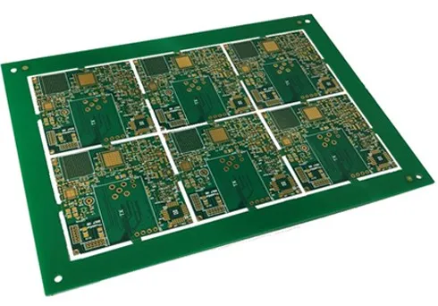
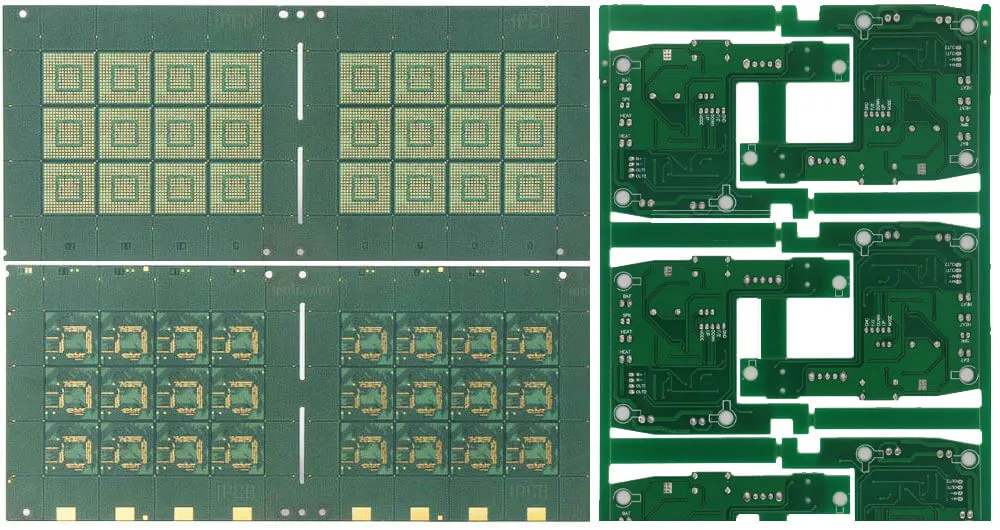
Before diving into the cost implications, let’s clarify what PCB panel size means. A PCB panel is a larger sheet of material, typically made of fiberglass or other substrates, on which multiple individual PCB designs are arranged for manufacturing. This process, known as panelization, allows manufacturers to produce several boards at once, improving efficiency.
The size of the panel can vary widely, often ranging from 9x12 inches to 18x24 inches or larger, depending on the manufacturer’s equipment and the project requirements. The choice of panel size isn’t arbitrary—it’s a critical decision that impacts material costs, production time, and even the quality of the final product.
Key Cost Drivers Linked to PCB Panel Size
When analyzing PCB panel size cost drivers, several factors come into play. Let’s break down the most significant ones to understand how they contribute to the overall expense of manufacturing.
1. Material Costs and PCB Panel Size
The most direct impact of PCB panel size is on material costs. Larger panels require more raw material, such as laminate and copper, which increases the upfront expense. For instance, a standard 18x24-inch panel might cost $50 in raw materials, while a smaller 9x12-inch panel could cost around $15. However, larger panels often allow for more individual boards to be produced in a single run, potentially reducing the per-unit material cost.
If a larger panel accommodates 20 individual PCBs while a smaller one only fits 5, the cost per board drops significantly with the larger panel. This is a key aspect of PCB panelization cost savings—maximizing the number of boards per panel to spread out material costs.
2. PCB Panel Size and Material Waste
While larger panels can lower per-unit costs, they can also lead to more material waste if not optimized. Material waste occurs when the panel layout doesn’t fully utilize the available space, leaving unused areas that are discarded after production. For example, if your individual PCB design is an irregular shape or has specific spacing requirements, a poorly planned panel layout might result in 20-30% of the material being wasted.
Waste directly translates to higher costs. If a panel costs $50 and 25% of it is unused, you’re effectively losing $12.50 per panel. Over thousands of panels, this adds up quickly. Optimizing PCB panel size for the lowest cost often involves working closely with your manufacturer to create efficient layouts that minimize waste.
3. Production Efficiency and Setup Costs
Panel size also affects production efficiency. Larger panels can reduce the number of setups required during manufacturing since more boards are processed at once. Each setup—where the production equipment is adjusted for a new panel—takes time and labor, adding to the cost. For example, processing 100 individual boards on five 9x12-inch panels might require five setups, while a single 18x24-inch panel holding 20 boards cuts setups down significantly.
Fewer setups mean lower labor costs and faster turnaround times. However, very large panels can sometimes be harder to handle or may require specialized equipment, which could offset some of these savings if the manufacturer isn’t equipped for them.
4. Tooling and Testing Expenses
Another factor in PCB panel size cost analysis is the impact on tooling and testing. Larger panels might require custom tooling or fixtures to hold them during production, especially for high-precision processes like drilling or routing. Additionally, testing multiple boards on a single panel can be more efficient, but if a defect is found in one board, it might affect the entire panel, leading to higher rejection rates and costs.
For instance, if a panel holds 10 boards and one fails during testing, you might lose the entire panel if the defect is due to a panel-wide issue like misalignment. Balancing panel size with testing efficiency is crucial for cost control.
Strategies for Optimizing PCB Panel Size for Lowest Cost
Now that we’ve covered the key cost drivers, let’s explore actionable strategies to optimize PCB panel size for the lowest cost. These tips can help you achieve significant savings while maintaining quality and efficiency.
1. Collaborate Early with Your Manufacturer
One of the most effective ways to optimize panel size is to involve your manufacturing partner early in the design process. They can provide insights into their standard panel sizes, equipment capabilities, and layout recommendations. For example, if their standard panel size is 18x24 inches, designing your board layout to fit efficiently within that dimension can avoid additional costs for custom panels or excessive waste.
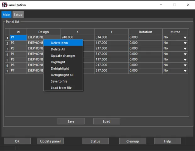
2. Use Panelization Software for Efficient Layouts
Modern design tools often include panelization features that help arrange multiple PCBs on a panel to minimize waste. These tools can calculate the best orientation and spacing, ensuring maximum utilization of the panel area. By reducing unused space from, say, 20% to 5%, you could save hundreds or thousands of dollars on large production runs.
3. Balance Panel Size with Production Volume
For small production runs, smaller panels might be more cost-effective since they reduce material waste and setup complexity. However, for high-volume orders, larger panels often provide better economies of scale. Analyze your production volume and choose a panel size that aligns with your needs. For instance, a run of 1,000 boards might benefit from 18x24-inch panels, while a prototype run of 10 boards could stick to a smaller 9x12-inch panel to keep costs low.
4. Consider Breakaway Tabs and Scoring
To further optimize space, consider using breakaway tabs or scoring lines to separate individual boards after production. This method allows you to fit boards closer together on the panel, reducing waste. However, ensure that the tabs or scoring don’t compromise the structural integrity of the boards during manufacturing or depanelization.
Real-World Examples of PCB Panelization Cost Savings
To illustrate the impact of panel size optimization, let’s look at two hypothetical scenarios based on common industry practices.
Scenario 1: Small Panel, High Waste
A company designs a small 9x12-inch panel for a run of 200 PCBs. Each panel holds only 4 boards due to spacing constraints, resulting in 50 panels total. With 20% material waste per panel and a cost of $15 per panel, the total material cost is $750, with $150 lost to waste. Additionally, 50 setups at $10 per setup add another $500, bringing the total to $1,250, or $6.25 per board.
Scenario 2: Larger Panel, Optimized Layout
The same company switches to an 18x24-inch panel costing $50 each, holding 16 boards per panel with only 5% waste. For 200 boards, they need 13 panels, costing $650 in materials with just $32.50 in waste. With only 13 setups at $10 each, setup costs are $130, bringing the total to $780, or $3.90 per board. That’s a savings of over 37% per board simply by optimizing panel size and layout.
These examples highlight how PCB panel size and material waste considerations can drastically affect the bottom line.
Common Pitfalls to Avoid in PCB Panel Size Selection
While optimizing panel size offers clear benefits, there are pitfalls to watch out for that can negate your efforts.
1. Ignoring Manufacturer Constraints
Choosing a panel size that doesn’t align with your manufacturer’s capabilities can lead to higher costs or delays. For instance, selecting a 24x36-inch panel when their equipment maxes out at 18x24 inches might require outsourcing or custom processing, driving up expenses.
2. Overloading Panels with Too Many Boards
While maximizing the number of boards per panel is ideal, overloading can lead to issues like insufficient spacing for tooling or testing, increasing the risk of defects. Always leave adequate margins for manufacturing tolerances—typically 0.1 to 0.2 inches between boards.
3. Neglecting Depanelization Challenges
Larger panels with many boards can be harder to depanelize, especially if the method (e.g., manual breaking or routing) isn’t suited to the design. Poor depanelization can damage boards, leading to higher rejection rates and costs.
Future Trends in PCB Panel Size and Cost Management for 2025
As we move into 2025, the PCB industry is evolving with new technologies and strategies for cost management. Based on recent industry insights, manufacturers are increasingly adopting automation and AI-driven tools for panel layout optimization, further reducing waste and setup times. Additionally, the push for sustainable practices is encouraging the use of recyclable materials and waste minimization techniques, which can influence panel size decisions.
Staying ahead of these trends can provide a competitive edge. For instance, leveraging AI tools to predict the most cost-effective panel size for a given design could become standard practice, saving both time and money.
Conclusion: Mastering PCB Panel Size for Cost Efficiency
In conclusion, PCB panel size plays a pivotal role in manufacturing cost, influencing everything from material usage to production efficiency. By understanding the key cost drivers—material costs, waste, setups, and tooling—you can make informed decisions to optimize your panel size for the lowest cost. Strategies like collaborating with manufacturers, using panelization software, and balancing panel size with production volume are essential for achieving PCB panelization cost savings.
Whether you’re working on a small prototype or a large-scale production run, paying attention to PCB panel size cost analysis can yield significant savings and improve project outcomes. Take the time to evaluate your panelization approach, and you’ll likely find opportunities to cut costs without compromising quality. At ALLPCB, we’re committed to helping you navigate these decisions with expert guidance and tailored solutions for your PCB needs.


